Chapter 3 of 10Chương 3/10 8 min8 phút
Stop 1: the idea and the designChặng 1: ý tưởng và thiết kế
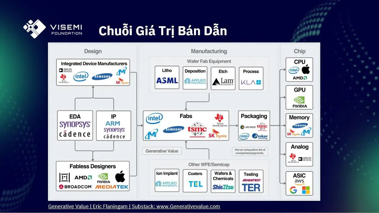
Before the A17 Pro was a piece of silicon, it was a design: about 19 billion transistors, laid out in software and checked again and again before a single wafer was made.3.1 This first stop on the chip’s journey is where that design comes from. Apple designed the chip, yet the software used to draw a chip like this, and some of the building blocks inside it, come from other companies.
Trước khi thành một mẩu silicon, con chip A17 Pro là một bản thiết kế. Khoảng 19 tỷ bóng bán dẫn (transistor) được sắp đặt trên phần mềm, kiểm tra đi kiểm tra lại, trước khi tấm wafer đầu tiên vào sản xuất.3.1 Chặng đầu tiên trên hành trình của con chip là nơi bản thiết kế ấy ra đời. Apple thiết kế con chip này, nhưng phần mềm để vẽ nên một con chip như thế, cùng một số khối dựng sẵn bên trong nó, đều đến từ những công ty khác.
In this chapter
Trong chương này
- Why a chip’s design starts from the job it must do
- What design software (EDA) and licensed building blocks (IP) are, and who sells them
- Why checking a design now takes as many engineers as drawing it
- How a finished design becomes a file the factory can use
- What designers and their software suppliers earn
- Vì sao việc thiết kế chip bắt đầu từ câu hỏi con chip phải làm gì
- Phần mềm thiết kế (EDA) và các khối dựng sẵn được mua bản quyền (IP) là gì, và ai bán chúng
- Vì sao ngày nay kiểm tra một bản thiết kế cần nhiều kỹ sư không kém việc vẽ ra nó
- Bản thiết kế hoàn chỉnh trở thành file để nhà máy sản xuất như thế nào
- Các công ty thiết kế và những hãng bán phần mềm cho họ kiếm được bao nhiêu
Chip design starts from what the chip must do
Thiết kế chip bắt đầu từ việc xác định con chip phải làm gì
Designing a chip starts the way designing any product does: with what it is for. A chip meant to compute very fast for AI will be a logic chip such as a GPU. One that must hold a great deal of data, a whole library of films, is a memory chip. A chip for 5G phones needs radio-frequency (RF) circuits. That purpose works like a compass: it decides which kind of chip to build and sets the direction for everything that follows, from research to manufacturing.
Thiết kế chip cũng bắt đầu như thiết kế bất cứ sản phẩm nào: từ câu hỏi nó dùng để làm gì. Muốn tính toán thật nhanh cho AI thì phải làm một chip logic, chẳng hạn GPU. Cần nhớ thật nhiều dữ liệu, như cả một kho phim, thì phải là chip nhớ. Chip cho điện thoại 5G lại cần mạch RF (radio frequency). Mục đích ấy giống như chiếc la bàn: nó quyết định sẽ làm loại chip nào và định hướng cho mọi việc về sau, từ nghiên cứu đến sản xuất.
That purpose goes into the chip’s specification, the document described in chapter 2. For the A17 Pro, the purpose was the iPhone 15 Pro itself. The chip is a system on chip (SoC): one piece of silicon that carries the phone’s six-core main processor, its CPU, together with a six-core GPU.3.2 It has to be fast, yet the only power it gets comes from a phone battery.
Mục đích ấy được ghi vào bản yêu cầu kỹ thuật (IC specification) của con chip, loại văn bản đã nói ở chương 2. Với A17 Pro, mục đích ấy chính là chiếc iPhone 15 Pro. Con chip này là một System on Chip (SoC): trên cùng một mẩu silicon có bộ xử lý chính sáu lõi của điện thoại, tức CPU, cùng một GPU sáu lõi.3.2 Nó phải chạy nhanh, trong khi nguồn điện duy nhất của nó chỉ là viên pin điện thoại.
Designers choose the architecture, then design in EDA software
Chọn kiến trúc chip rồi thiết kế bằng phần mềm EDA
With the purpose fixed, the designers decide the chip’s architecture: the top-level plan of which blocks it contains, such as processor cores, graphics cores and memory controllers, and how they connect. At chip companies such as NVIDIA or Intel, that choice belongs to the company’s own designers, and it shapes what the chip will be good at.
Khi mục đích đã rõ, người thiết kế quyết định kiến trúc chip: bản kế hoạch tổng thể cho biết con chip gồm những khối nào, như lõi xử lý, lõi đồ họa, bộ điều khiển bộ nhớ, và các khối ấy nối với nhau ra sao. Ở những công ty chip như NVIDIA hay Intel, lựa chọn này nằm trong tay đội thiết kế của công ty, và nó định hình thế mạnh của con chip sau này.
Chips now hold billions of transistors, so no team could place them one at a time; an NVIDIA Blackwell GPU holds 208 billion.3.3 Designers work in electronic design automation (EDA) software, programs that turn a description of the circuit into a layout, the drawing of the chip, and check it at every step. That software comes from a few companies, among them Synopsys, Cadence and Siemens EDA. In July 2025 Synopsys also bought the simulation-software maker Ansys.3.4, 3.5
Chip ngày nay có tới hàng tỷ transistor, nên không đội kỹ sư nào đặt nổi từng cái một; một GPU Blackwell của NVIDIA chứa tới 208 tỷ.3.3 Người thiết kế làm việc bằng EDA (phần mềm thiết kế chip), loại chương trình chuyển bản mô tả mạch thành layout, tức bản vẽ con chip, và kiểm tra nó ở từng bước. Phần mềm này đến từ một vài công ty, trong đó có Synopsys, Cadence và Siemens EDA. Tháng 7/2025, Synopsys còn mua lại hãng phần mềm mô phỏng Ansys.3.4, 3.5
EDA companies are software companies: they sell the tools a chip is designed with. They also work closely with the chipmakers, because a design is only worth something if it can be made, and it has to be checked against the way each chipmaker actually builds its chips.
Các hãng EDA là công ty phần mềm: họ bán công cụ để thiết kế chip. Họ cũng làm việc sát sao với các nhà sản xuất chip, vì bản thiết kế chỉ có giá trị khi sản xuất được, mà muốn vậy thì phải kiểm tra nó theo đúng cách từng nhà sản xuất chế tạo chip trên thực tế.
Building blocks you license: IP
Những khối dựng sẵn được mua bản quyền: IP
Designers rarely start from nothing either. A modern chip reuses a great deal of intellectual property (IP): ready-made pieces of design, licensed from the companies that created them. Think of them as Lego bricks. Companies such as Arm, Synopsys and Cadence develop these pieces and test them until they are known to work, and chip companies build their own designs out of them. Each licensed block, a processor core, say, or the circuit that runs a USB port, is called an IP core.
Người thiết kế cũng hiếm khi bắt đầu từ con số không. Một con chip hiện đại dùng lại rất nhiều IP (khối thiết kế mua bản quyền): những phần thiết kế làm sẵn, mua quyền sử dụng từ công ty đã tạo ra chúng. Cứ hình dung chúng như những viên gạch Lego. Các công ty như Arm, Synopsys hay Cadence phát triển những khối này và thử đi thử lại cho tới khi chắc chắn chúng chạy đúng, còn các công ty chip thì dùng chúng để xây nên thiết kế của mình. Mỗi khối mua bản quyền như thế, chẳng hạn một lõi xử lý hay mạch điều khiển cổng USB, gọi là một IP core.
Reuse has a limit, though. Every chip company reuses as much proven IP as it can, yet it still needs parts of its own that make its chip different, the way a house built from standard materials still has to suit the family who live in it. That is why companies working with the same EDA tools and much of the same IP still turn out very different chips: Intel is known for its CPUs, NVIDIA for its GPUs.
Dùng lại cũng có giới hạn. Công ty chip nào cũng tận dụng tối đa những IP đã được kiểm nghiệm, song vẫn cần những phần do chính mình làm ra để tạo nét riêng cho con chip. Một ngôi nhà xây bằng vật liệu tiêu chuẩn cũng vậy, rốt cuộc vẫn phải hợp với gia đình sống trong đó. Vì vậy mà dù cùng dùng một bộ công cụ EDA và nhiều IP giống nhau, các công ty vẫn làm ra những con chip rất khác nhau: Intel nổi tiếng với CPU, còn NVIDIA với GPU.
The A17 Pro shows both sides. Apple designs the chip itself, yet the processor inside it is built on Arm’s architecture, used under licence, like more than 99% of the world’s smartphone processors.3.6, 3.7, 3.8
A17 Pro cho thấy cả hai mặt ấy. Apple tự thiết kế con chip, nhưng bộ xử lý bên trong dựa trên kiến trúc của Arm, dùng theo giấy phép, giống như hơn 99% bộ xử lý điện thoại thông minh trên thế giới.3.6, 3.7, 3.8
Replacing these companies is hard. The EDA firms and Arm are few, and they are woven into the way nearly every chip is designed and made, so a newcomer is unlikely to unseat them. In one chip designer’s view, the way in is narrower: new IP for particular uses, above all for the newest technology nodes, the latest generations of manufacturing process, where fresh building blocks are still needed.
Thay thế những công ty này không dễ. Các hãng EDA và Arm vốn đã ít, lại gắn chặt vào cách người ta thiết kế và sản xuất gần như mọi con chip, nên một công ty mới khó lòng soán ngôi họ. Theo góc nhìn của một người làm thiết kế chip, cơ hội chen chân hẹp hơn thế: làm ra IP mới cho những mục đích riêng, nhất là cho các tiến trình bán dẫn (technology node) mới nhất. Đó là những thế hệ quy trình sản xuất tiên tiến nhất, nơi vẫn cần những khối dựng mới.
Checking whether the design works as specified
Kiểm định xem thiết kế có hoạt động đúng yêu cầu không
A chip’s design is the work of two kinds of engineer: one creates the design, and the other checks, again and again, that it does what the specification says. A design engineer builds it, in several steps. In logic synthesis, software turns the engineers’ written description of the circuit into a network of logic gates. Physical design then turns the gates into the exact shapes that will be printed, starting with floor planning, which arranges the chip’s large blocks on its surface.
Bản thiết kế một con chip là công sức của hai loại kỹ sư: một bên làm ra thiết kế, một bên kiểm tra hết lần này đến lần khác xem nó có chạy đúng như yêu cầu kỹ thuật hay không. Kỹ sư thiết kế dựng nên nó qua nhiều bước. Ở bước tổng hợp logic (synthesis), phần mềm chuyển bản mô tả mạch do kỹ sư viết ra thành một mạng cổng logic. Sau đó, bước physical design biến các cổng logic thành những hình vẽ chính xác sẽ “in” lên wafer, bắt đầu từ floor planning, bước sắp xếp các khối lớn của chip trên bề mặt.
Checking that the design works is verification, the job of the verification engineer, and it starts as soon as a design exists, even half-finished. Verification engineers build test setups and run simulations of the design, hunting for the mistakes that would otherwise show up only once the chip had been made, when a fix means redesigning it and making it all over again.
Việc kiểm tra xem thiết kế có chạy đúng hay không gọi là kiểm định (verification), phần việc của verification engineer, tức kỹ sư verification. Công việc này bắt đầu ngay khi vừa có bản thiết kế, dù còn dở dang. Các kỹ sư này dựng môi trường thử và chạy mô phỏng bản thiết kế, săn tìm những lỗi mà nếu bỏ sót thì chỉ lộ ra khi chip đã làm xong, lúc ấy muốn sửa là phải thiết kế lại và sản xuất lại từ đầu.
| Design engineer | Verification engineer | |
|---|---|---|
| The question | How should the circuit be built? | Does it do what the specification says? |
| The work | Writing the design, synthesis, floor planning, physical design | Building test setups, running simulations, hunting for mistakes |
| When | From the architecture to the final layout | From the first draft of the design to the hand-over to the factory |
| Kỹ sư thiết kế | Kỹ sư verification | |
|---|---|---|
| Câu hỏi | Nên dựng mạch thế nào? | Nó có làm đúng như yêu cầu kỹ thuật không? |
| Công việc | Viết thiết kế, tổng hợp logic, floor planning, physical design | Dựng môi trường thử, chạy mô phỏng, săn lỗi |
| Giai đoạn | Từ kiến trúc đến bản layout cuối cùng | Từ bản nháp thiết kế đầu tiên đến lúc bàn giao cho nhà máy |
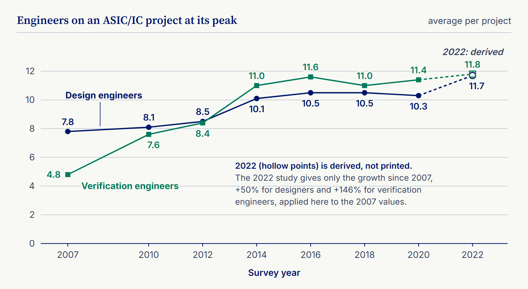
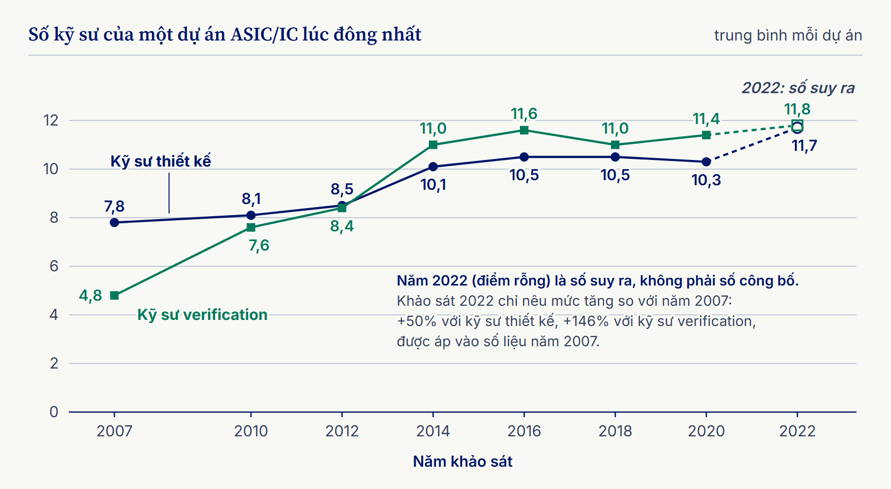
The second job has grown faster. In surveys by Siemens EDA and the Wilson Research Group, the average chip project at its peak had about 8 design engineers and 5 verification engineers in 2007, and about 12 of each by 2022; since 2014, verification engineers have matched or outnumbered designers.3.9, 3.10 The more complex the chip and the more advanced its process, the more there is to check, and the checking has not got easier. In the 2024 survey only 14% of projects got the chip right on the first manufacturing run, with no redesign needed; in the 2026 survey, only 5% did.3.11, 3.12
Số người làm công việc thứ hai tăng nhanh hơn. Theo các cuộc khảo sát của Siemens EDA và Wilson Research Group, một dự án chip trung bình lúc đông người nhất có khoảng 8 kỹ sư thiết kế và 5 kỹ sư verification vào năm 2007. Đến năm 2022, mỗi bên có khoảng 12 người, và từ năm 2014, số kỹ sư verification luôn bằng hoặc vượt số kỹ sư thiết kế.3.9, 3.10 Chip càng phức tạp, quy trình sản xuất càng tiên tiến thì càng nhiều thứ phải kiểm tra, và việc kiểm tra không hề dễ đi. Trong khảo sát năm 2024, chỉ 14% dự án làm đúng con chip ngay từ lần sản xuất đầu tiên, không phải thiết kế lại; đến khảo sát năm 2026, con số ấy chỉ còn 5%.3.11, 3.12
Much of this checking still needs people. Tools, AI among them, may take over part of it in time, but for now verification needs many engineers. It is also why large chip companies hand some of their verification and physical design to the smaller design houses of chapter 2. That is a kind of outsourcing: work outside the core goes to outside firms. Chapter 9 looks at what that demand means for Vietnam.
Phần lớn việc kiểm tra này vẫn cần đến con người. Các công cụ, kể cả AI, rồi có thể gánh bớt một phần, nhưng hiện nay verification vẫn cần rất nhiều kỹ sư. Đó cũng là lý do các công ty chip lớn giao một phần verification và physical design cho những design house nhỏ hơn đã nói ở chương 2, tức những hãng nhận thiết kế thuê. Đây cũng là một kiểu outsourcing (thuê ngoài): phần việc không cốt lõi được giao cho công ty bên ngoài. Chương 9 sẽ bàn xem nhu cầu ấy có ý nghĩa gì với Việt Nam.
The finished design is saved as a GDS file and sent to the fab
Bản thiết kế hoàn chỉnh được lưu thành file GDS rồi gửi tới nhà máy
After many stages, the design reaches its final form: a GDS file, the standard file format for chip drawings, holding the exact shapes of every layer of the chip. Handing that file over to be made is called tape-out. It is the moment the design leaves the designers’ hands and goes to the fab.
Qua rất nhiều công đoạn, bản thiết kế đạt tới dạng cuối cùng: một file GDS, định dạng chuẩn cho bản vẽ chip, chứa hình dạng chính xác của từng lớp trên con chip. Việc bàn giao file ấy để đưa vào sản xuất gọi là tape-out. Đó là lúc bản thiết kế rời tay người thiết kế để đến nhà máy sản xuất chip (fab).
For the A17 Pro, the file went to TSMC, a foundry: a company that makes chips to other companies’ designs. TSMC made it on its 3 nm process, known as N3B.3.13 Before a single layer could be printed, though, the fab needed the raw material the chip is built on, and that is the next stop.
Với A17 Pro, file được gửi tới TSMC, một foundry, tức công ty chuyên sản xuất chip theo thiết kế của công ty khác. TSMC làm con chip này ở tiến trình 3 nm, gọi là N3B.3.13 Nhưng trước khi in được lớp đầu tiên, fab cần đến thứ nguyên liệu để dựng con chip lên, và đó là chặng tiếp theo.
What this stop earns
Giá trị kinh tế được tạo ra ở công đoạn này
Design is where more than half of a chip’s value is added.3.14 The table below reads as chapter 2 explained: what the segment sold, then its gross margin. The fabless companies design chips without factories of their own, and the ten largest of them took in about US$250 billion in 2024. The firms that sell them software and IP are far smaller, about US$19 billion together, yet they keep more of each dollar of revenue than any other part of the industry, because software is written once and sold many times.
Thiết kế là khâu tạo ra hơn một nửa giá trị gia tăng của một con chip.3.14 Bảng dưới đây đọc theo cách chương 2 đã hướng dẫn: mảng này bán được bao nhiêu, rồi đến biên lợi nhuận gộp. Các công ty fabless thiết kế chip nhưng không có nhà máy; riêng mười công ty lớn nhất trong số đó thu về khoảng 250 tỷ USD trong năm 2024. Những hãng bán phần mềm và IP cho họ nhỏ hơn nhiều, gộp lại chỉ khoảng 19 tỷ USD, vậy mà trên mỗi đồng doanh thu họ giữ lại được nhiều hơn mọi mảng khác trong ngành, vì phần mềm viết một lần mà bán được nhiều lần.
| Stop 1 | The idea and the design |
|---|---|
| What the segment sold (2024) | The ten largest fabless chip designers: about US$250 billion.3.15 Design software (EDA) and IP: about US$19 billion.3.16 |
| Gross margin | Design software and IP: 80 to 97% (Synopsys 80%, Cadence 86%, Arm 97%). Fabless designers: about 50 to 75%, from MediaTek’s 50% to NVIDIA’s 75% (2024).3.17 |
| How many big players | Design software: three (Synopsys, which bought Ansys in July 2025; Cadence; Siemens EDA). Processor architecture: Arm’s is used in more than 99% of phone processors. Chip designers: no world count; China alone had about 3,600 design firms in 2024.3.18 |
| What it means for you | Verification teams have grown faster than design teams (plate 3.1). In one practitioner’s view, design is a good place to start because it needs people more than capital: its main cost is a team of good engineers, not a factory. |
| Chặng 1 | Ý tưởng và thiết kế |
|---|---|
| Mảng này bán được bao nhiêu (2024) | Mười công ty fabless lớn nhất: khoảng 250 tỷ USD.3.15 Phần mềm thiết kế (EDA) và IP: khoảng 19 tỷ USD.3.16 |
| Biên lợi nhuận gộp | Phần mềm thiết kế và IP: 80 đến 97% (Synopsys 80%, Cadence 86%, Arm 97%). Công ty fabless: khoảng 50 đến 75%, từ 50% của MediaTek đến 75% của NVIDIA (2024).3.17 |
| Có bao nhiêu công ty lớn | Phần mềm thiết kế: ba hãng (Synopsys, đã mua lại Ansys vào tháng 7/2025; Cadence; Siemens EDA). Kiến trúc bộ xử lý: kiến trúc của Arm có mặt trong hơn 99% bộ xử lý điện thoại. Công ty thiết kế chip: chưa ai đếm trên toàn thế giới; riêng Trung Quốc có khoảng 3.600 công ty năm 2024.3.18 |
| Điều này có ý nghĩa gì với bạn | Đội verification tăng nhanh hơn đội thiết kế (hình 3.1). Theo góc nhìn của một người trong nghề, thiết kế là điểm khởi đầu tốt vì cần con người hơn là vốn: chi phí chính là một đội kỹ sư giỏi, chứ không phải một nhà máy. |