Chapter 3 of 9Chương 3/9 6 min6 phút
How a chip is madeChip được sản xuất như thế nào
A chip begins as a computer file and ends as a slab of silicon carrying billions of working transistors. Somewhere between the two, a designer hands over a drawing, and a foundry has to turn it into matter.
Một con chip bắt đầu từ một tập tin và kết thúc bằng một tấm silicon mang hàng tỷ bóng bán dẫn (transistor) đang hoạt động. Ở khoảng giữa, người thiết kế bàn giao một bản vẽ, và foundry phải biến bản vẽ ấy thành vật thể thật.
In this chapter
Trong chương này
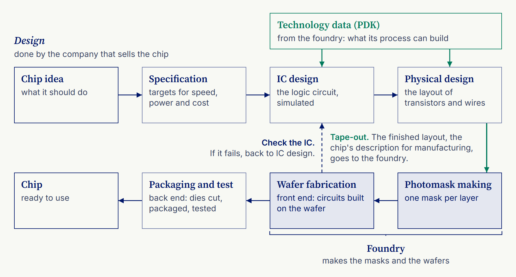
- Which stages a chip passes through from idea to finished product, and where the foundry takes over
- Why a chip is like a high-rise building, with a mask for every floor
- What a photomask is, and why one set can cost millions of dollars
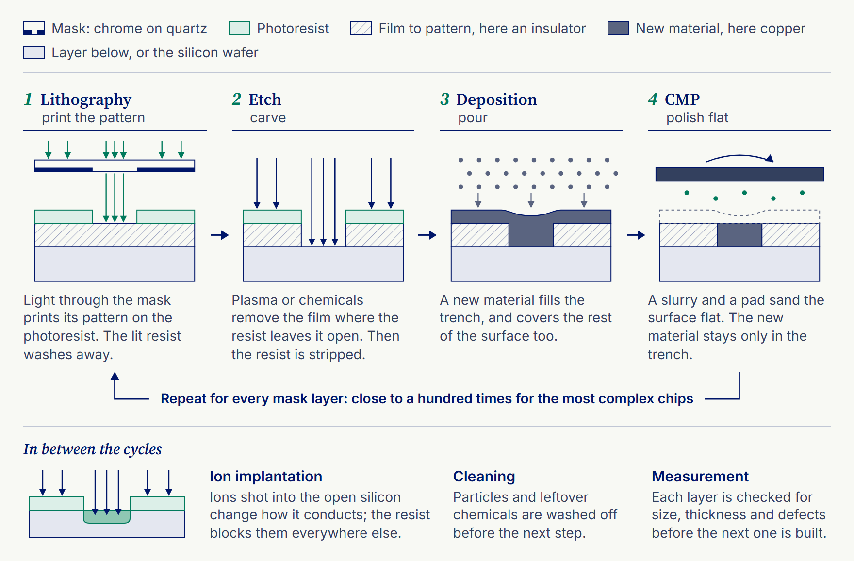
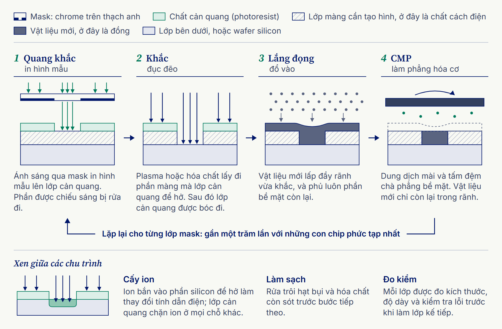
- How the four steps of lithography, etch, deposition and CMP repeat for every layer
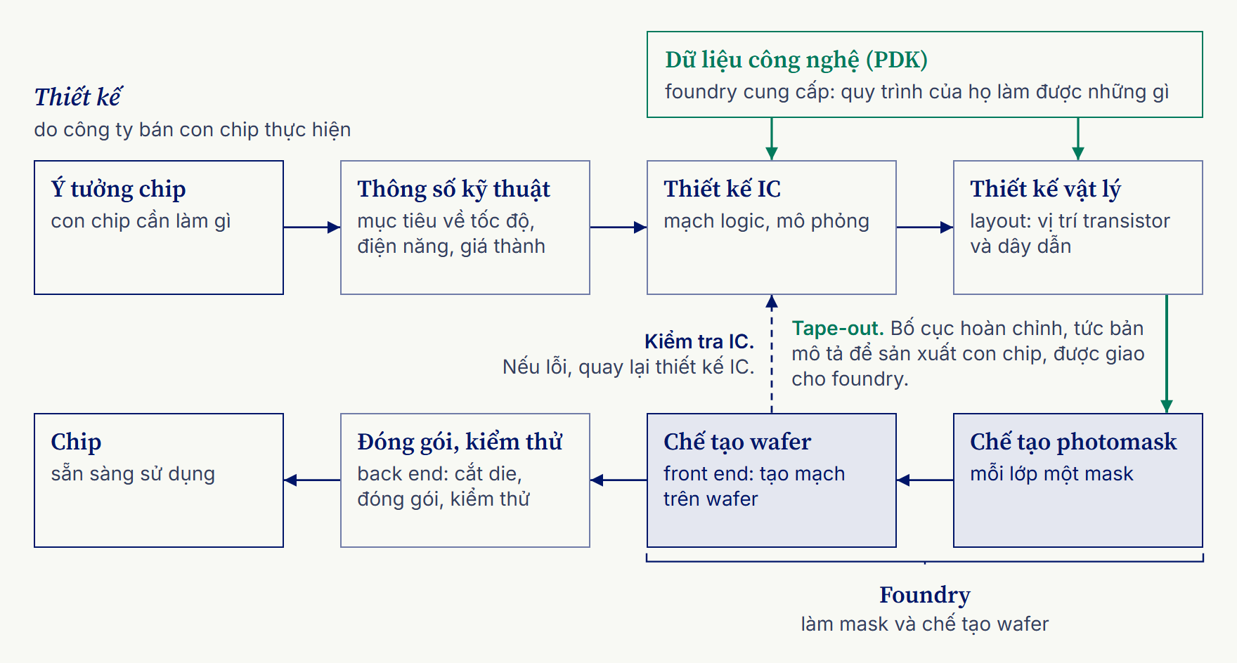
- Con chip đi từ ý tưởng đến thành phẩm qua những chặng nào, và foundry tiếp quản từ công đoạn nào
- Vì sao một con chip giống một tòa nhà cao tầng, mà tầng nào cũng cần mask riêng
- Photomask là gì, và vì sao một bộ mask có thể tốn hàng triệu đô la
- Bốn bước quang khắc, khắc, lắng đọng và CMP lặp lại qua từng lớp ra sao
A chip goes from idea to tape-out
Con chip đi từ ý tưởng đến tape-out
Long before manufacturing starts, the two sides are already talking. The foundry provides a Process Design Kit (PDK): the technical data describing what its process can build. The designer works inside those rules, first designing the circuit, then the physical layout: arranging transistors and wiring so the chip is as small, fast, and power-efficient as possible. The finished layout is handed to the foundry at tape-out, and from that moment the drawing starts becoming a physical object: photomasks first, then patterned wafers, then packaged and tested chips.
Rất lâu trước khi sản xuất bắt đầu, hai bên đã trao đổi với nhau. Foundry cung cấp một Process Design Kit (PDK): dữ liệu kỹ thuật mô tả những gì quy trình của họ có thể chế tạo. Người thiết kế làm việc trong khuôn khổ những quy tắc đó, trước tiên thiết kế mạch, rồi đến bố cục vật lý: sắp xếp transistor và dây dẫn sao cho con chip nhỏ nhất, nhanh nhất và tiết kiệm điện năng nhất có thể. Khâu bàn giao bố cục hoàn chỉnh cho foundry gọi là tape-out, và từ lúc đó bản vẽ bắt đầu trở thành vật thể thật: trước tiên là photomask, rồi đến wafer đã tạo hình, rồi đến những con chip đã đóng gói và kiểm tra.
A modern chip is like a high-rise building
Con chip hiện đại giống một tòa nhà cao tầng
Building a chip is often compared to building a house: draw the blueprint, dig and pour the foundation, raise the walls, run the electricity and plumbing, then finish the surfaces. A modern chip, though, is less a house than a high-rise. At the bottom sits the device layer, the Front End of Line (FEOL), where the transistors live. Above it rise many floors of copper wiring, the Back End of Line (BEOL), connecting the transistors into working logic.3.1 Stretched out, the copper inside one chip would run for hundreds of kilometers.
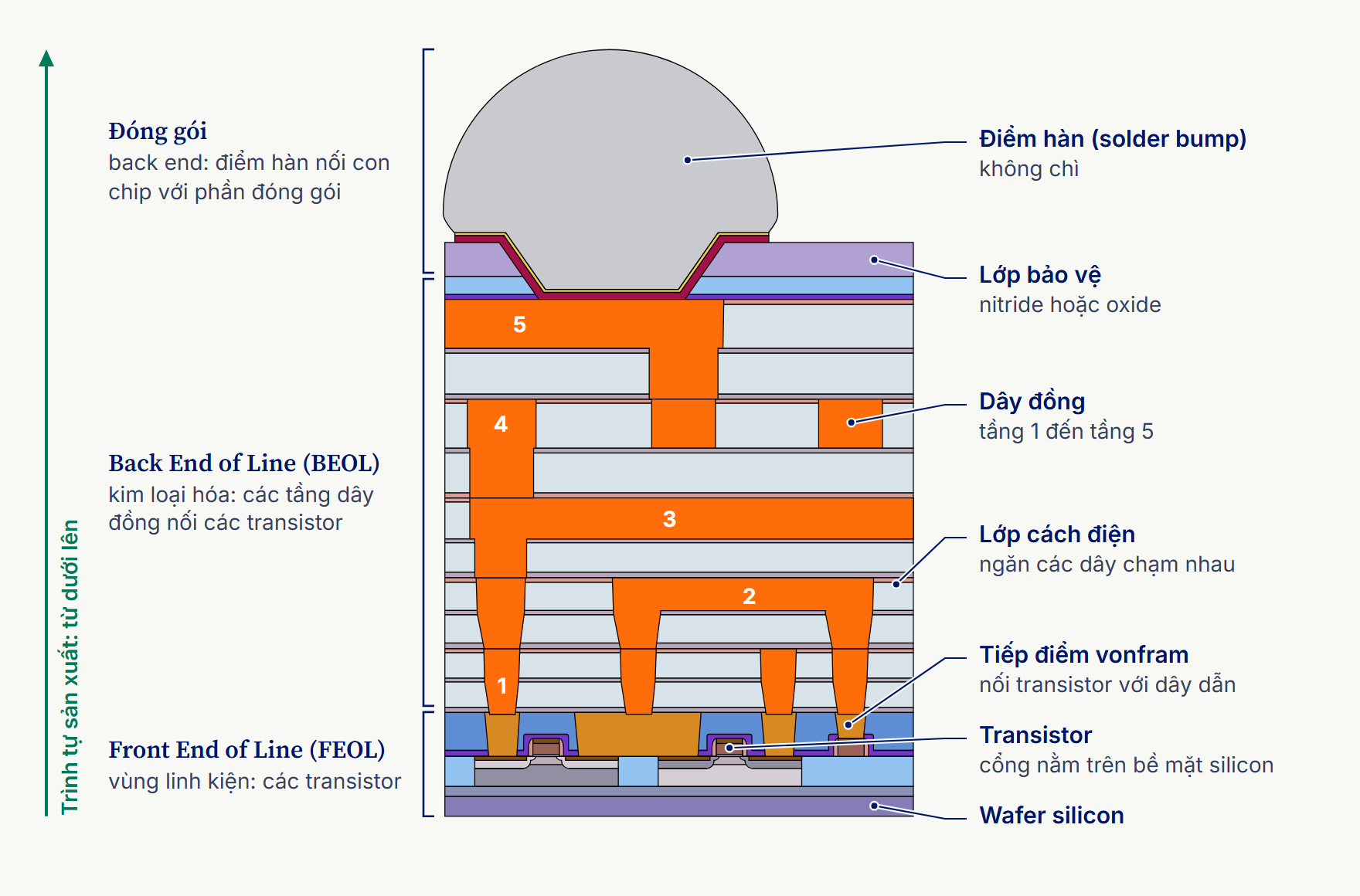
Chế tạo một con chip thường được ví với việc xây một ngôi nhà: lên bản thiết kế, đào và đổ móng, dựng tường, đi điện nước, rồi hoàn thiện bề mặt. Có điều, con chip hiện đại giống một tòa nhà cao tầng hơn là một căn nhà. Ở đáy là lớp linh kiện, Front End of Line (FEOL), nơi đặt các transistor. Bên trên nó mọc lên nhiều tầng dây đồng, Back End of Line (BEOL), nối các transistor lại với nhau để chạy được các mạch logic.3.1 Nếu kéo thẳng ra, dây đồng trong một con chip dài tới hàng trăm cây số.
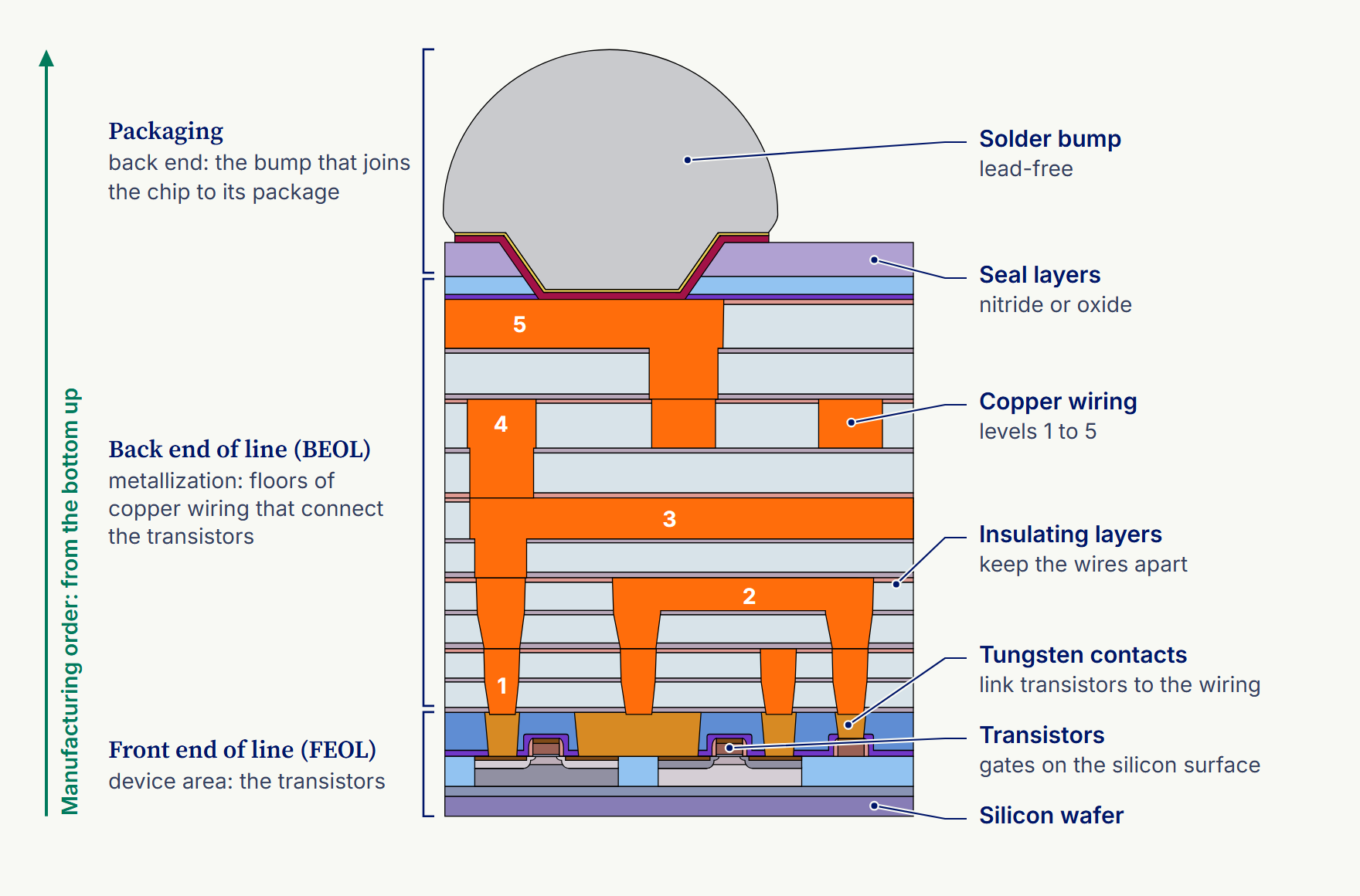
An advanced CPU can stack close to twenty such floors, and every floor needs its own photomask, sometimes several: one mask may finish only the living room, and the kitchen needs another. The full journey, from bare silicon to the final wiring level, is what takes four months (chapter 1).
Một CPU tiên tiến có thể chồng gần hai mươi tầng như vậy, và mỗi tầng cần photomask riêng, đôi khi là vài chiếc: một mask có thể chỉ hoàn thiện phòng khách, còn nhà bếp lại cần một chiếc khác. Đi trọn hành trình ấy, từ silicon trần đến tầng dây dẫn cuối cùng, mất chừng bốn tháng (chương 1).
Why a mask set costs millions of dollars
Vì sao một bộ mask có giá hàng triệu đô la
A full mask set takes around two to three weeks to produce, and that work, not the cheap raw material, is what costs millions. A photomask is the mold of one layer. The foundry splits the layout into layers, checks and simulates each one, and writes each mask with an electron beam, much as an office laser printer puts shapes on a sheet of paper, only far more slowly, because the beam has to trace every shape in turn. A simple two-transistor CMOS circuit already needs six masks; a complex chip like NVIDIA’s H100 or Apple’s A18 needs close to one hundred. A full set costs from a few million dollars at mature nodes to tens of millions of dollars for the most advanced chips.
Làm một bộ mask đầy đủ mất khoảng hai đến ba tuần, và chính công sức ấy, chứ không phải nguyên liệu vốn rẻ, mới khiến cả bộ tốn hàng triệu đô la. Photomask là chiếc “khuôn” của một lớp. Foundry tách bố cục thành từng lớp, kiểm tra và mô phỏng từng lớp, rồi in từng mask bằng một chùm tia điện tử (electron beam). Cách in này giống như máy in laser ở văn phòng in hình lên giấy, chỉ có điều chậm hơn rất nhiều, vì chùm tia phải vẽ lần lượt từng hình. Một mạch CMOS hai transistor đơn giản đã cần đến sáu mask; một con chip phức tạp như H100 của NVIDIA hay A18 của Apple cần gần một trăm chiếc. Chi phí cho cả bộ đi từ vài triệu đô la ở các tiến trình bán dẫn (node) đã hoàn thiện đến hàng chục triệu đô la cho những con chip tiên tiến nhất.
A basic mask is just a plate of quartz carrying a thin, patterned layer of chrome. A mask for EUV, the most advanced kind of lithography, is far harder to make: it is a mirror, built from about forty pairs of alternating molybdenum and silicon layers on a glass that barely expands with heat, each layer controlled to extreme precision. The layout must also be fine-tuned on supercomputers, sometimes for a week per mask, so that what lands on the wafer matches what the designer drew. The frontier of this work is computational: starting from the shape wanted on the wafer and computing backwards what the mask must look like.
Một mask cơ bản chỉ là một tấm thạch anh mang một lớp chrome mỏng đã được tạo hình. Mask cho EUV, loại quang khắc tiên tiến nhất, khó làm hơn nhiều: đó là một tấm gương. Gương này gồm khoảng bốn mươi cặp lớp molypden và silicon xếp xen kẽ, đặt trên một nền thủy tinh gần như không giãn nở vì nhiệt, lớp nào cũng phải kiểm soát đến độ chính xác cực cao. Bố cục còn phải được tinh chỉnh trên siêu máy tính, có khi mất cả tuần cho một mask, để những gì in xuống wafer khớp với những gì người thiết kế đã vẽ. Hướng đi mới nhất là thiết kế ngược, dựa vào tính toán: bắt đầu từ hình dạng mong muốn trên wafer, rồi tính ngược lại xem mask phải trông như thế nào.
What happens if a photomask has a defect?Điều gì xảy ra nếu một photomask có lỗi?
Flaws on the mask itself are caught while it is being written. Small ones are repaired in place, using an electron beam to deposit material exactly where the flaw is, and a mask that cannot be repaired is written again. Other defects show up only on the wafer, where light interference distorts the printed pattern, so measurement tools check the surface after each etch. Defects within tolerance are accepted. A pattern that keeps printing wrong and hurts the chip’s performance sends the team back to the design step: the mask data is corrected and the mask is made again.
Lỗi trên chính mask được phát hiện ngay trong lúc in mask. Lỗi nhỏ được sửa tại chỗ, bằng cách dùng chùm tia điện tử để lắng đọng vật liệu vào đúng chỗ lỗi; mask nào không sửa được thì phải in lại từ đầu. Có những lỗi khác chỉ lộ ra trên wafer, khi giao thoa ánh sáng làm méo hình đã in, nên sau mỗi lần khắc đều có máy đo kiểm tra lại bề mặt. Lỗi nằm trong dung sai cho phép thì được chấp nhận. Còn nếu một hình mẫu cứ in sai và làm giảm hiệu năng con chip thì phải quay lại bước thiết kế, sửa dữ liệu mask và làm lại photomask.
Every mask layer goes through the same four-step cycle
Mỗi lớp mask đều trải qua cùng một chu trình bốn bước
Each mask layer is built in the same four steps, and lithography comes first. With the mask ready, it projects the pattern onto the wafer, shrinking it on the way, much as a phone camera fits a twenty-story building onto its screen. Today’s lithography machines shrink it exactly four times; older generations shrank it five or ten times. A 300 mm wafer carries many small dies, each one a future chip with billions of transistors, so the same pattern is repeated across the whole surface.
Lớp mask nào cũng được làm theo cùng bốn bước, và quang khắc là bước đầu tiên. Khi mask đã sẵn sàng, bước này chiếu hình mẫu trên mask lên wafer, đồng thời thu nhỏ hình mẫu ấy, giống như khi ta dùng điện thoại chụp một tòa nhà hai mươi tầng: trên màn hình, cả tòa nhà chỉ còn bé xíu. Máy quang khắc ngày nay thu nhỏ đúng bốn lần; các thế hệ máy cũ hơn thu nhỏ năm hoặc mười lần. Một wafer 300 mm mang nhiều die nhỏ, mỗi die về sau sẽ thành một con chip với hàng tỷ transistor, nên cùng một hình mẫu được lặp lại trên khắp bề mặt.
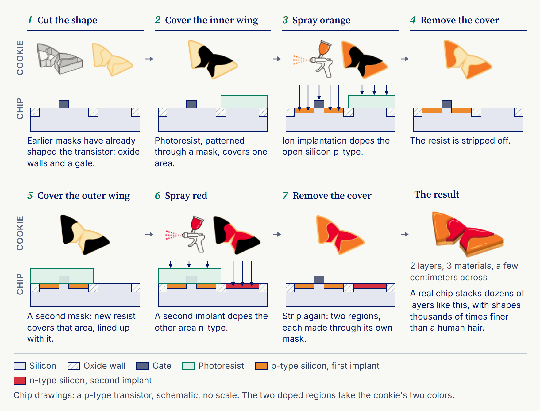
Then the building starts, in three more moves. Etch carves: a gas or chemical removes the material exactly where the photoresist, the light-sensitive coating that lithography has just patterned, leaves it exposed. Deposition pours: a new material fills the carved space, and spills over everything else too. So chemical mechanical planarization (CMP) polishes: a slurry and a pad sand the surface flat, keeping the new material only where it belongs. Litho, etch, deposit, polish: this cycle repeats for every mask layer, close to a hundred times for the most complex chips. With cleaning, ion implantation and measurement steps in between, the whole flow runs to more than a thousand steps, floor by floor, until the high-rise is complete.
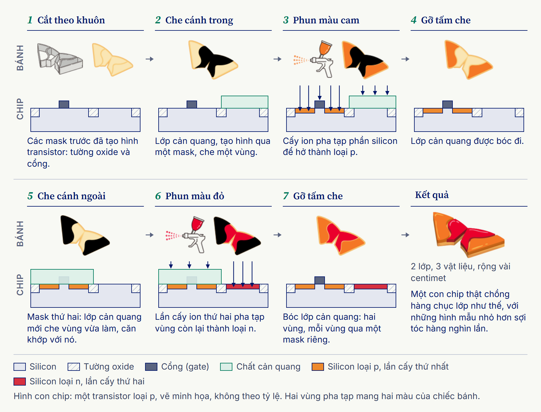
Rồi việc xây dựng bắt đầu, qua ba thao tác tiếp theo. Khắc là bước “đục đẽo”: một chất khí hoặc hóa chất phản ứng với vật liệu và lấy đi đúng phần mà lớp chất cản quang (photoresist), lớp phủ nhạy sáng vừa được quang khắc tạo hình, để hở. Lắng đọng là bước “đổ vào”: một vật liệu mới lấp đầy chỗ vừa khắc, và tràn lên cả phần bề mặt còn lại. Vì vậy cần thêm bước làm phẳng hóa cơ (CMP) để đánh bóng: một dung dịch mài (slurry) và một tấm đệm chà phẳng bề mặt, chỉ giữ vật liệu mới ở đúng chỗ cần có. Quang khắc, khắc, lắng đọng, đánh bóng: chu trình này lặp lại cho từng lớp mask, gần một trăm lần với những con chip phức tạp nhất. Cộng thêm các bước làm sạch, cấy ion và đo kiểm xen giữa, cả quy trình lên tới hơn một nghìn bước, hết tầng này đến tầng khác, cho đến khi tòa nhà cao tầng hoàn tất.