Chapter 2 of 9Chương 2/9 7 min7 phút
Moore's Law and the evolution of the transistorĐịnh luật Moore và sự tiến hóa của transistor
What does the “3 nm” on a new phone’s spec sheet actually measure? The answer starts sixty years ago, with a promise made by Intel co-founder Gordon Moore that the whole industry has been racing to keep ever since.
Con số “3 nm” trong bảng thông số của một chiếc điện thoại mới thật ra đo cái gì? Câu trả lời bắt đầu từ sáu mươi năm trước, từ một lời hứa của Gordon Moore, nhà đồng sáng lập Intel, mà cả ngành bán dẫn đã chạy theo suốt từ đó đến nay.
In this chapter
Trong chương này
- What Moore’s Law says, and what doubling every two years really implies
- The breakthroughs that kept scaling alive, from strained silicon to EUV and GAA
- Why a node name like 3 nm no longer measures anything on the chip
- How the transistor went from flat to 3D: FinFET, GAAFET, and the CFET idea
- Định luật Moore nói gì, và việc tăng gấp đôi sau mỗi hai năm có ý nghĩa gì trong thực tế
- Những đột phá giúp quá trình thu nhỏ không dừng lại, từ strained silicon đến EUV và GAA
- Vì sao tên node như 3 nm không còn đo kích thước thật nào trên chip
- Bóng bán dẫn (transistor) đã chuyển từ cấu trúc phẳng sang 3D như thế nào: FinFET, GAAFET và ý tưởng CFET

About every two years, the number of transistors on a chip doubles
Cứ khoảng hai năm, số transistor trên chip lại tăng gấp đôi
Moore's Law says that the number of transistors on a chip doubles about every two years. It is not a law of physics but an observation: in 1965 Gordon Moore noticed that the transistor count on an integrated circuit was doubling about every year, and in 1975 he revised it to the roughly two-year pace still quoted today.2.1, 2.2 In practical terms: each generation packs in more transistors, which has historically meant faster chips, while the manufacturing cost per transistor falls. That observation became the industry’s metronome, because it captures what the market keeps demanding: higher density, higher performance, lower cost.
Theo Định luật Moore, số bóng bán dẫn (transistor) trên một con chip cứ khoảng hai năm lại tăng gấp đôi. Đây không phải định luật vật lý mà là một quan sát: năm 1965, Gordon Moore nhận thấy số transistor trên một vi mạch tăng gấp đôi khoảng mỗi năm một lần, và đến năm 1975 ông điều chỉnh lại thành nhịp khoảng hai năm, con số vẫn được nhắc đến cho tới nay.2.1, 2.2 Nói cho dễ hình dung: mỗi thế hệ chip chứa nhiều transistor hơn, trước nay điều đó thường đồng nghĩa với chip chạy nhanh hơn, trong khi chi phí sản xuất mỗi transistor giảm xuống. Quan sát ấy đã thành nhịp chuẩn cho cả ngành, vì nó phản ánh đúng điều thị trường luôn đòi hỏi: mật độ cao hơn, hiệu năng cao hơn, chi phí thấp hơn.
Doubling sounds gentle until it keeps compounding. Recall the old chessboard puzzle: one grain of rice on the first square, and twice as many on each square after. The first few squares hold almost nothing, but by the 64th the board holds hundreds of billions of tonnes of rice. Staying on that curve took, in almost every era, a new breakthrough in materials or structure.
Tăng gấp đôi nghe có vẻ nhẹ nhàng, cho đến khi nó cứ thế nhân lên mãi. Hãy nhớ bài toán hạt thóc trên bàn cờ: ô đầu một hạt, mỗi ô sau gấp đôi ô trước. Vài ô đầu chẳng đáng kể, nhưng đến ô thứ 64 thì cả bàn cờ đã chứa hàng trăm tỷ tấn thóc. Để bám được đường cong đó, gần như thời kỳ nào ngành cũng phải có một đột phá mới về vật liệu hoặc cấu trúc.
The breakthroughs that kept Moore's Law going
Những đột phá giữ nhịp Định luật Moore
Each time scaling hit a wall, the industry changed something fundamental: first the materials inside the transistor, then the light used to print it, and finally the shape of the transistor itself.
Mỗi lần quá trình thu nhỏ đụng phải “bức tường”, ngành công nghiệp lại thay đổi một điều căn bản: trước tiên là vật liệu bên trong transistor, rồi đến ánh sáng dùng để in nó, và cuối cùng là chính hình dạng của transistor.
| Year | Breakthrough | Why it mattered |
|---|---|---|
| 2003 | Strained SiGe | Mechanical strain in the silicon channel raises carrier mobility, so transistors switch faster |
| 2007 | High-k Metal Gate (HKMG) | Replaces the traditional SiO2 gate dielectric and cuts gate leakage |
| Around 2007 | Immersion lithography | A liquid between lens and wafer raises the machine’s resolution (Intel adopted it at 32 nm in 2010) |
| 2012 | FinFET | The first 3D transistor structure enters production, at Intel’s 22 nm |
| 2019 | EUV lithography | The printing wavelength drops from 193 nm to 13.5 nm, a huge step forward by ASML |
| 2022 | Gate-All-Around (GAA) | The gate wraps the channel completely; first brought to production by Samsung |
| 2010s onward | Advanced packaging | Performance gains from combining chips, not only from shrinking them |
| Năm | Đột phá | Vì sao nó quan trọng |
|---|---|---|
| 2003 | Strained silicon (SiGe chịu ứng suất) | Ứng suất cơ học trong kênh dẫn silicon làm tăng độ linh động của hạt tải điện, nhờ đó transistor chuyển mạch nhanh hơn |
| 2007 | High-k Metal Gate (HKMG) | Thay thế lớp điện môi cổng SiO2 truyền thống, giảm dòng rò qua cổng |
| Khoảng 2007 | Quang khắc nhúng | Một lớp chất lỏng giữa thấu kính và wafer giúp tăng độ phân giải của máy (Intel áp dụng từ node 32 nm năm 2010) |
| 2012 | FinFET | Cấu trúc transistor 3D đầu tiên đi vào sản xuất, ở node 22 nm của Intel |
| 2019 | Quang khắc EUV | Bước sóng ánh sáng dùng để in giảm từ 193 nm xuống 13,5 nm, một bước tiến vượt bậc của ASML |
| 2022 | Gate-All-Around (GAA) | Cổng bao bọc hoàn toàn kênh dẫn; Samsung là hãng đầu tiên đưa vào sản xuất |
| Từ thập niên 2010 trở đi | Đóng gói tiên tiến (advanced packaging) | Hiệu năng tăng nhờ kết hợp các chip, chứ không chỉ nhờ thu nhỏ chúng |
Node names today are only generation labels
Tên node ngày nay chỉ còn là nhãn đánh dấu thế hệ
In the early planar era the node name roughly matched a real dimension: the transistor’s gate length. From the late 1990s the printed gate was already shorter than the name (about 50 nm at the 90 nm node, for example), and from the FinFET generation onward the name stopped tracking any single feature. A modern node name like 3 nm, 2 nm, or 14 angstrom measures nothing on the chip; a literal 10 angstrom would span only about four silicon atoms. The names survive as generation labels: each new node still promises a meaningful jump in density, performance, or energy efficiency.
Ở giai đoạn đầu của thời transistor phẳng, tên tiến trình bán dẫn (node) gần tương đương với một kích thước thật: chiều dài cổng (gate length) của transistor. Từ cuối thập niên 1990, cổng in ra trên chip đã ngắn hơn con số trong tên gọi (chẳng hạn ở node 90 nm, cổng chỉ dài khoảng 50 nm), và từ thế hệ FinFET trở đi, tên node không còn gắn với bất kỳ chi tiết nào. Tên node hiện đại như 3 nm, 2 nm hay 14 angstrom không đo thứ gì trên chip; nếu đúng là 10 angstrom thì chỉ dài khoảng bốn nguyên tử silicon. Ngày nay các tên gọi ấy chỉ còn là nhãn đánh dấu thế hệ: mỗi node mới vẫn hứa hẹn một bước tiến đáng kể về mật độ, hiệu năng hoặc hiệu quả năng lượng.
Do the numbers in 5 nm or 3 nm mean anything at all?Vậy những con số trong 5 nm hay 3 nm có ý nghĩa gì không?
Not as a measurement. They drifted away from the gate length during the planar era, and since 22 nm, the first FinFET generation, they have not matched any feature at all. Today they work like model years for cars: a shorthand for one generation of process technology.
Không, nếu coi đó là số đo. Chúng đã tách dần khỏi chiều dài cổng ngay trong thời transistor phẳng, và từ node 22 nm, thế hệ FinFET đầu tiên, thì không còn khớp với chi tiết nào nữa. Ngày nay chúng giống như đời xe ô tô (xe đời 2024, đời 2025): một cách gọi tắt cho từng thế hệ công nghệ sản xuất.
The transistor went from flat to 3D
Transistor chuyển từ cấu trúc phẳng sang cấu trúc 3D
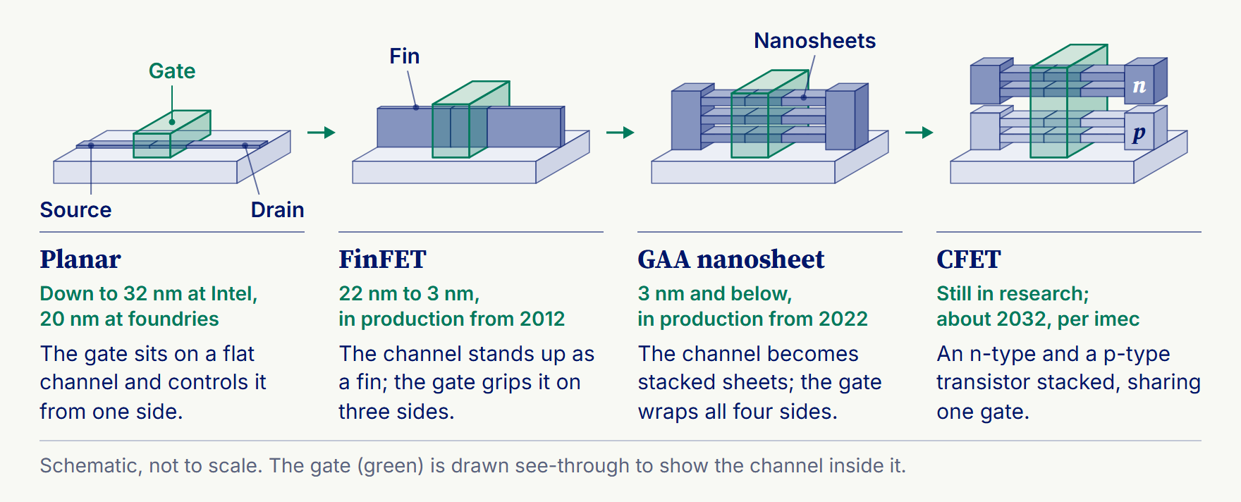
The classical planar transistor is a flat switch: current flows from source to drain, and a gate on top opens or closes the channel. Shrink it too far and the gate can no longer close the channel completely, so current leaks even when the switch is off. The high-k metal gate stopped a different leak, current tunnelling through the ever-thinner gate insulator, but the leak through the channel remained, and below a certain size the flat shape itself was the problem.
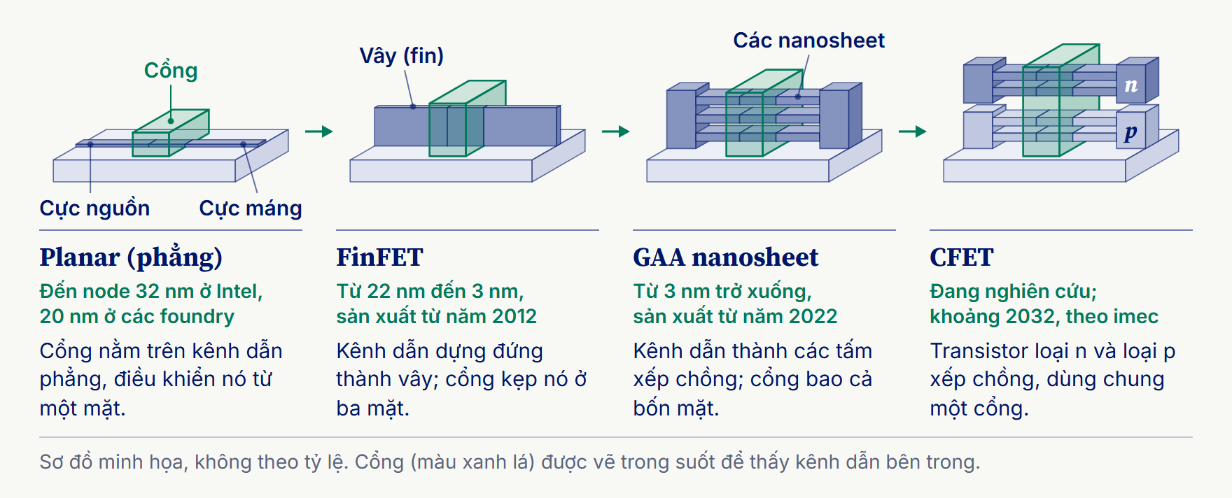
Transistor phẳng cổ điển là một “công tắc” nằm ngang: dòng điện chạy từ cực nguồn (source) sang cực máng (drain), còn cổng ở phía trên thì mở hoặc đóng kênh dẫn (channel). Thu nhỏ quá mức thì cổng không còn đóng kín kênh dẫn được nữa, nên dòng điện vẫn rò qua ngay cả khi công tắc đã tắt. High-k metal gate chặn được một dòng rò khác, dòng điện xuyên hầm qua lớp cách điện của cổng vốn ngày càng mỏng, nhưng dòng rò qua kênh dẫn vẫn còn, và dưới một kích thước nhất định, chính hình dạng phẳng mới là vấn đề.
The answer was to build upward. In a FinFET the channel stands up like a fin and the gate grips it on three sides, giving far better control: less leakage, and more performance at lower power. FinFETs run today’s AMD Ryzen processors, NVIDIA graphics chips, and the PlayStation 5. One step further, Gate-All-Around (GAA) wraps the channel on all four sides and stacks several nanosheets on top of each other, so more current simply means stacking more channels. GAA is the transistor of the newest leading-edge processes (Samsung’s 3 nm, TSMC’s 2 nm, Intel’s 18A), and the first chips built on them are only now reaching the market.
Câu trả lời là xây lên cao. Trong FinFET, kênh dẫn dựng đứng như một chiếc vây và cổng kẹp lấy nó ở ba mặt, nhờ đó kiểm soát tốt hơn nhiều: ít dòng rò hơn, hiệu năng cao hơn mà lại tốn ít điện hơn. FinFET có mặt trong các bộ xử lý AMD Ryzen, chip đồ họa NVIDIA và máy PlayStation 5 ngày nay. Tiến thêm một bước, Gate-All-Around (GAA) bao bọc kênh dẫn ở cả bốn mặt và xếp chồng nhiều nanosheet lên nhau, nên muốn tăng dòng điện, chỉ cần xếp thêm kênh dẫn. GAA là transistor của các node tiên tiến nhất hiện nay (Samsung 3 nm, TSMC 2 nm, Intel 18A), và những con chip đầu tiên làm trên các node này mới bắt đầu ra thị trường.
After GAA, transistors may be stacked on top of each other
Sau GAA, bước tiếp theo có thể là xếp chồng transistor lên nhau
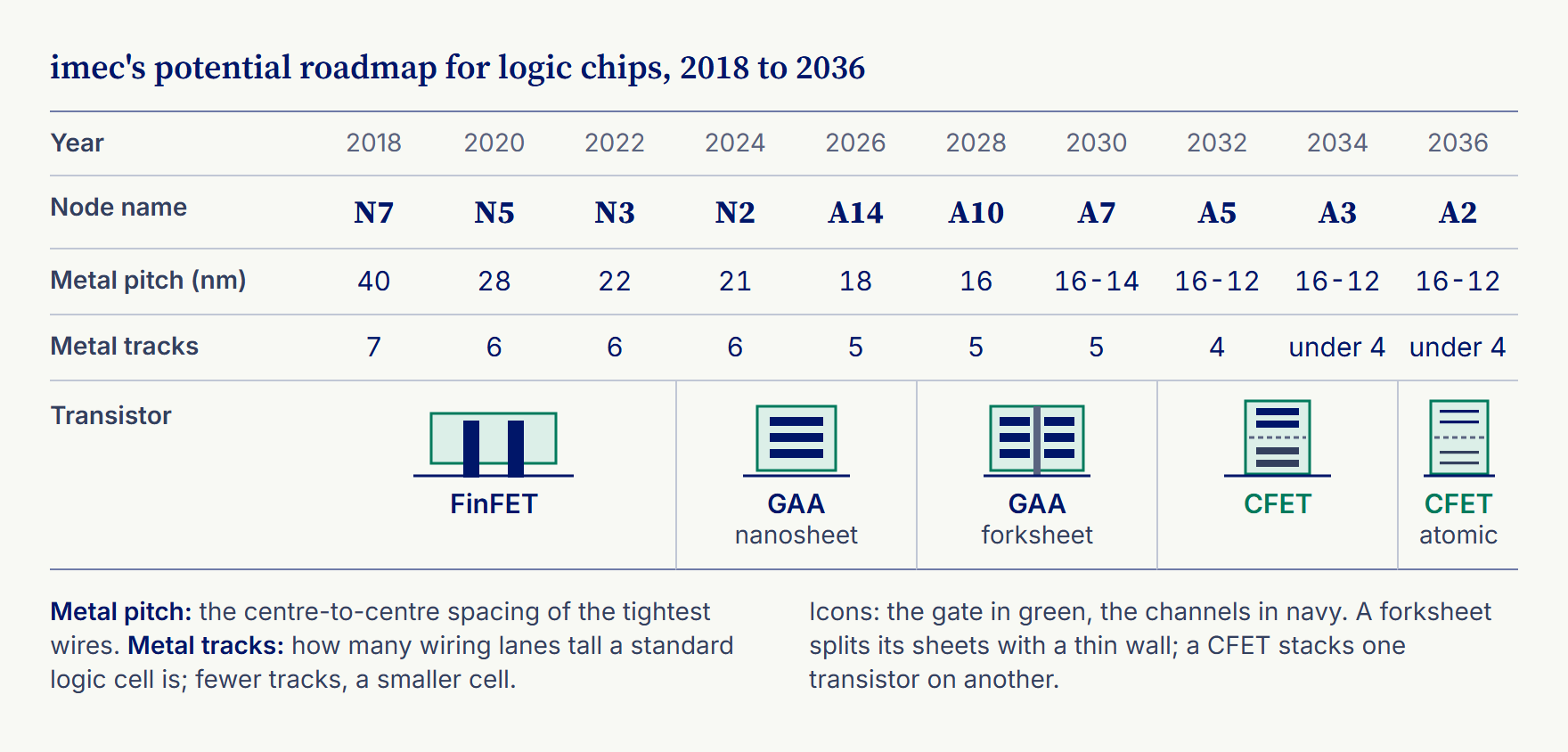
The next idea on the table is the Complementary FET (CFET): take the two kinds of transistor that every chip uses in pairs, NMOS and PMOS, stack one directly on top of the other, and let them share one gate. Density goes up, the wires between them get shorter, and power drops. Research roadmaps, like the one published by the Belgian research center imec, sketch the path: FinFET through N3, GAA nanosheets and then forksheets until around 2030, and CFET from the A5 generation, around 2032.2.3 CFET is still in research and development, not yet in production.
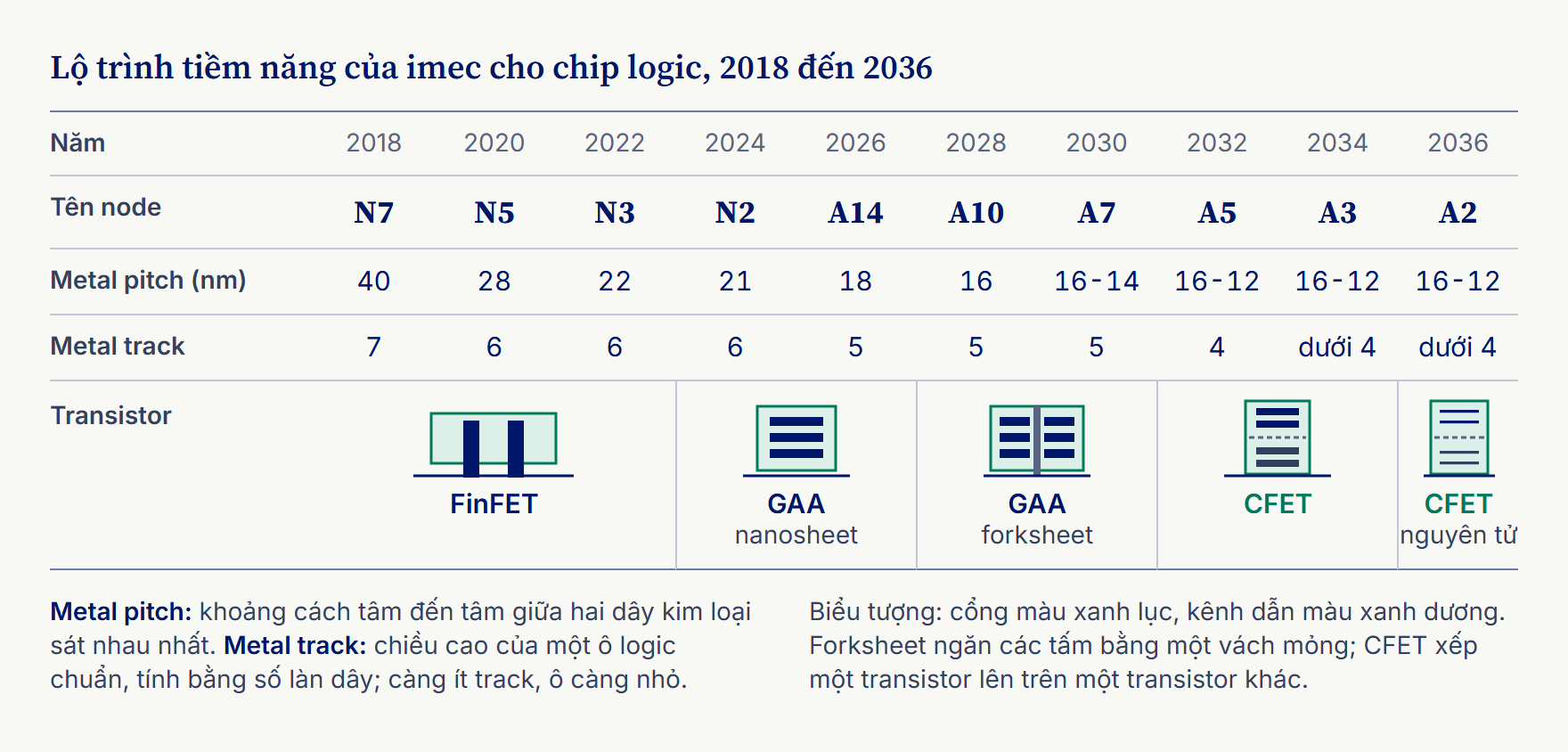
Ý tưởng tiếp theo đang được bàn đến là Complementary FET (CFET): lấy hai loại transistor mà chip nào cũng dùng theo cặp, NMOS và PMOS, xếp cái này trực tiếp lên trên cái kia và cho chúng dùng chung một cổng. Mật độ tăng lên, dây nối giữa chúng ngắn lại, và điện năng tiêu thụ giảm xuống. Các lộ trình nghiên cứu, như lộ trình do trung tâm nghiên cứu imec của Bỉ công bố, phác ra con đường: FinFET đến hết N3, GAA nanosheet rồi forksheet đến khoảng năm 2030, và CFET từ thế hệ A5, khoảng năm 2032.2.3 CFET vẫn đang trong giai đoạn nghiên cứu và phát triển, chưa đi vào sản xuất.
And the material underneath it all is still silicon. Graphene and III-V materials appear regularly in university labs, but nothing yet looks ready to replace silicon in production within the next five to ten years.
Và vật liệu nền tảng bên dưới tất cả vẫn là silicon. Graphene và các vật liệu nhóm III-V vẫn thường được nghiên cứu trong phòng thí nghiệm của các trường đại học, nhưng trong vòng năm đến mười năm tới, chưa có vật liệu nào có vẻ đủ sức thay thế silicon trong sản xuất.