Chapter 9 of 10Chương 9/10 9 min9 phút
Beyond communicationKhông chỉ để truyền tin
The same photonics that makes, steers and detects light for communication is starting to do other jobs, in cars that measure the road ahead with laser pulses and in lenses thin enough to make on a wafer. Everything in this book so far has followed one signal: made on a chip, carried by fiber across oceans and through data centers, and switched beside the rack. This chapter steps off that road.
Quang tử học (photonics) tạo ra, điều khiển và thu nhận ánh sáng để truyền tin, nhưng cũng chính công nghệ ấy đang bắt đầu nhận những việc khác. Nó có mặt trên những chiếc ô tô đo con đường phía trước bằng xung laser, và trong những thấu kính mỏng đến mức có thể chế tạo ngay trên wafer. Các chương trước đều đi theo một tín hiệu duy nhất: sinh ra trên chip, theo sợi quang vượt đại dương và đi qua các trung tâm dữ liệu (data center), rồi qua bộ chuyển mạch ngay bên tủ máy. Chương này rẽ sang một nhánh khác.
In this chapter
Trong chương này
- How LIDAR measures distance by timing a pulse of light
- Why smart glasses need a tiny, bright display and very light optics
- How a curved glass lens bends light, and why phone cameras still stick out
- How a flat layer of tiny nanostructures bends light instead
- Where flat lenses are headed next, and where they still fall short
- LIDAR đo khoảng cách bằng cách bấm giờ một xung ánh sáng như thế nào
- Vì sao kính thông minh cần một màn hình nhỏ mà sáng, cùng hệ quang học thật nhẹ
- Thấu kính thủy tinh cong bẻ cong ánh sáng ra sao, và vì sao camera điện thoại vẫn lồi lên
- Một lớp phẳng gồm những cấu trúc nano tí hon bẻ cong ánh sáng ra sao
- Thấu kính phẳng sắp được dùng vào đâu, và còn thua kém ở điểm nào
LIDAR helps a self-driving car measure distance with light
LIDAR giúp xe tự lái đo khoảng cách bằng ánh sáng
A self-driving car has to know, many times a second, where everything around it is. One approach leans on ordinary cameras and AI chips, much as a human driver relies on eyes and a brain. A camera, though, records a flat picture, and the distance to the car ahead has to be inferred from it. LIDAR measures that distance directly, with light.
Trong mỗi giây, một chiếc xe tự lái phải xác định nhiều lần xem mọi thứ quanh nó đang ở đâu. Có một cách dựa vào camera thông thường và chip AI, giống như người lái xe dựa vào mắt và bộ não. Nhưng camera chỉ ghi lại một hình ảnh phẳng, và khoảng cách tới chiếc xe phía trước phải suy ra từ hình ảnh ấy. LIDAR thì đo trực tiếp khoảng cách đó, bằng ánh sáng.
The principle is called time of flight. The lidar fires a short pulse of laser light, the pulse bounces off an object, and a light sensor catches the reflection. A timer measures how long the round trip took. Light covers about 30 centimeters in a billionth of a second, so the distance is simply the speed of light multiplied by that time, then halved, because the light went there and back. An object 30 meters away sends its echo back after about 200 nanoseconds, 200 billionths of a second.
Nguyên lý này gọi là thời gian bay (time of flight). LIDAR phát ra một xung laser ngắn, xung ấy dội lại khi gặp vật thể, và một cảm biến quang bắt lấy ánh sáng phản xạ. Một bộ đếm thời gian đo xem chuyến đi và về ấy mất bao lâu. Trong một phần tỷ giây, ánh sáng đi được khoảng 30 centimet, nên khoảng cách chỉ đơn giản là tốc độ ánh sáng nhân với thời gian đo được, rồi chia đôi, vì ánh sáng phải đi rồi quay lại. Một vật cách xe 30 mét sẽ gửi tín hiệu dội về sau khoảng 200 nano giây, tức 200 phần tỷ giây.
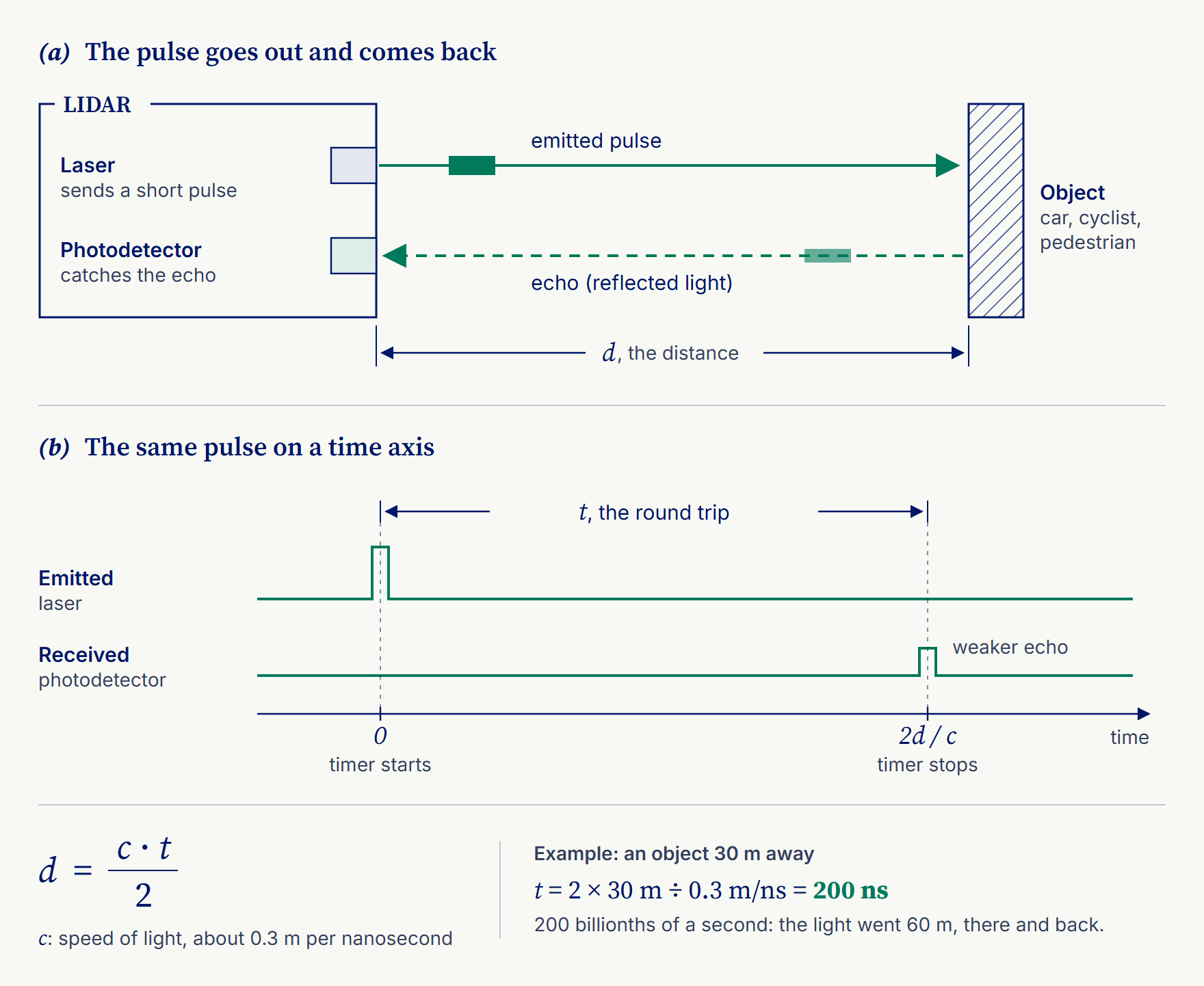
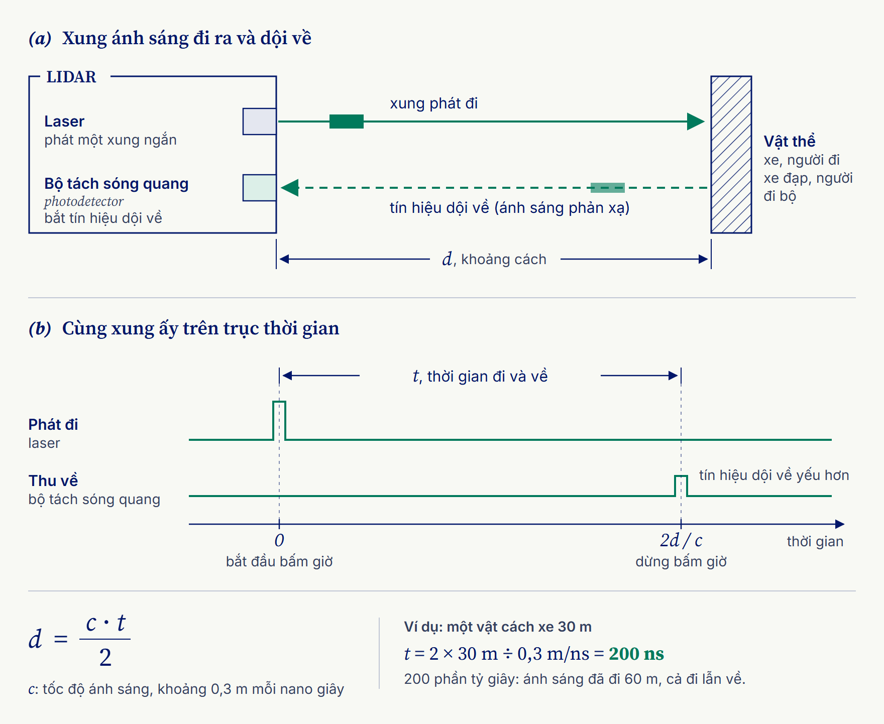
One pulse gives one distance. Sweep a great many pulses across the scene and each echo becomes a point with its own position in three dimensions, part of a cloud of points.9.1 Together they make a 3D map of the street, accurate to within centimeters. Repeat the measurement and the map also shows how fast each car, cyclist or pedestrian is moving, so the car can adjust its own speed in good time.
Một xung cho một khoảng cách. Quét thật nhiều xung khắp khung cảnh, mỗi tín hiệu dội về sẽ thành một điểm có vị trí riêng trong không gian ba chiều. Các điểm ấy họp thành một “đám mây điểm”.9.1 Gộp lại, chúng tạo thành bản đồ 3D của con phố, chính xác đến từng centimet. Lặp lại phép đo, bản đồ còn cho biết từng chiếc xe, người đi xe đạp hay người đi bộ đang di chuyển nhanh đến đâu, để xe kịp điều chỉnh tốc độ của mình.
Robotaxis such as Waymo’s already carry several lidars. The company’s fifth-generation system, introduced in 2020, put a 360-degree lidar on the roof that sees more than 300 meters and added short-range lidars at four points around the car to cover blind spots close by, alongside cameras and radar.9.2 Later generations have changed the layout again, but the idea stays the same: a laser source, optics that steer the beam, and a photodetector that catches the echo. These are the three stages of an optical link from chapter 2.
Những chiếc taxi tự lái như của Waymo đã mang theo vài bộ LIDAR. Hệ thống thế hệ thứ năm của hãng ra mắt năm 2020 với một bộ LIDAR quét 360 độ trên nóc xe, nhìn xa hơn 300 mét. Bốn vị trí quanh thân xe có thêm các bộ LIDAR tầm ngắn để phủ những điểm mù ở gần, bên cạnh camera và radar.9.2 Các thế hệ về sau lại thay đổi cách bố trí thêm lần nữa, nhưng ý tưởng vẫn vậy: một nguồn laser, hệ quang học “lái” chùm tia, và một bộ tách sóng quang (photodetector) bắt lấy tín hiệu dội về. Đó cũng chính là ba công đoạn của một đường truyền quang ở chương 2.
Smart glasses show text and pictures right in front of the eyes
Kính thông minh hiện chữ và hình ngay trước mắt người đeo
The second near-term use is augmented and virtual reality, AR/VR, including smart glasses that show text and pictures right in front of the eyes. Today the phone is where most people look things up and call their family on video. Several large technology companies are betting that such glasses will take over part of that job. In augmented reality they can also lay virtual objects over the real street, the way a game can drop a Pokémon onto the pavement in front of you.
Ứng dụng thứ hai trong tương lai gần là thực tế tăng cường và thực tế ảo, gọi chung là AR/VR, trong đó có những chiếc kính thông minh hiện chữ và hình ngay trước mắt người đeo. Ngày nay, chiếc điện thoại là nơi phần lớn mọi người tra cứu thông tin và gọi video cho người thân. Nhiều công ty công nghệ lớn đang đặt cược vào loại kính này, tin rằng chúng sẽ gánh một phần việc đó. Với thực tế tăng cường, kính còn có thể đặt những vật thể ảo chồng lên con phố thật, như khi một trò chơi thả một chú Pokémon xuống vỉa hè trước mặt bạn.
Glasses set two hard problems for light. The display has to be tiny and still bright enough to read in daylight. Many phones and smartwatches today use an OLED screen. MicroLEDs, built from III-V semiconductors, the same family of materials as the lasers in chapter 4, promise to be brighter, more efficient and longer-lived than OLEDs, which suits glasses worn outdoors.9.3 The optics have to be light and thin enough to wear all day, too, and that is where the lens itself comes in.
Kính thông minh đặt ra hai bài toán quang học khó. Màn hình phải thật nhỏ nhưng vẫn đủ sáng để đọc giữa ban ngày. Nhiều điện thoại và đồng hồ thông minh hiện nay dùng màn hình OLED (organic light-emitting diode). MicroLED làm từ bán dẫn III-V, cùng họ vật liệu với các con laser ở chương 4. Loại màn hình này hứa hẹn sáng hơn, hiệu quả hơn và bền hơn OLED, rất hợp với kính đeo ra ngoài trời.9.3 Hệ quang học cũng phải đủ nhẹ và mỏng để đeo suốt ngày, và đến đây thì chính chiếc thấu kính trở thành vấn đề.
After four hundred years, the curved lens still works the same way
Sau bốn trăm năm, thấu kính cong vẫn hoạt động theo cùng một nguyên lý
Every camera, telescope and pair of glasses rests on one idea, and it is old. The telescopes of the early 1600s, Galileo’s among them, focused light with a curved piece of glass, and the lenses in a phone camera, mostly molded plastic today, still work the same way. The principle is refraction: light slows down when it passes from air into glass, and changes direction at the boundary. How much it slows is given by the material’s refractive index, about 1 for air and higher for glass. Shape the glass so that it is thicker in the middle than at the edges, and every ray bends toward the same point, the focus.
Mọi chiếc camera, kính thiên văn hay cặp kính đeo mắt đều dựa trên một ý tưởng, và ý tưởng ấy đã rất cũ. Những chiếc kính thiên văn đầu thế kỷ 17, trong đó có chiếc của Galileo, hội tụ ánh sáng bằng một miếng thủy tinh cong, và những thấu kính trong camera điện thoại, nay phần lớn làm bằng nhựa đúc, vẫn làm việc theo đúng nguyên lý ấy. Nguyên lý ở đây là khúc xạ: ánh sáng chậm lại khi đi từ không khí vào thủy tinh, và đổi hướng ngay tại mặt phân cách. Ánh sáng chậm đi bao nhiêu là do chiết suất (refractive index) của vật liệu quyết định: không khí có chiết suất xấp xỉ 1, thủy tinh cao hơn. Tạo hình miếng thủy tinh sao cho phần giữa dày hơn phần rìa, mọi tia sáng sẽ cùng hội tụ về một điểm, gọi là tiêu điểm.
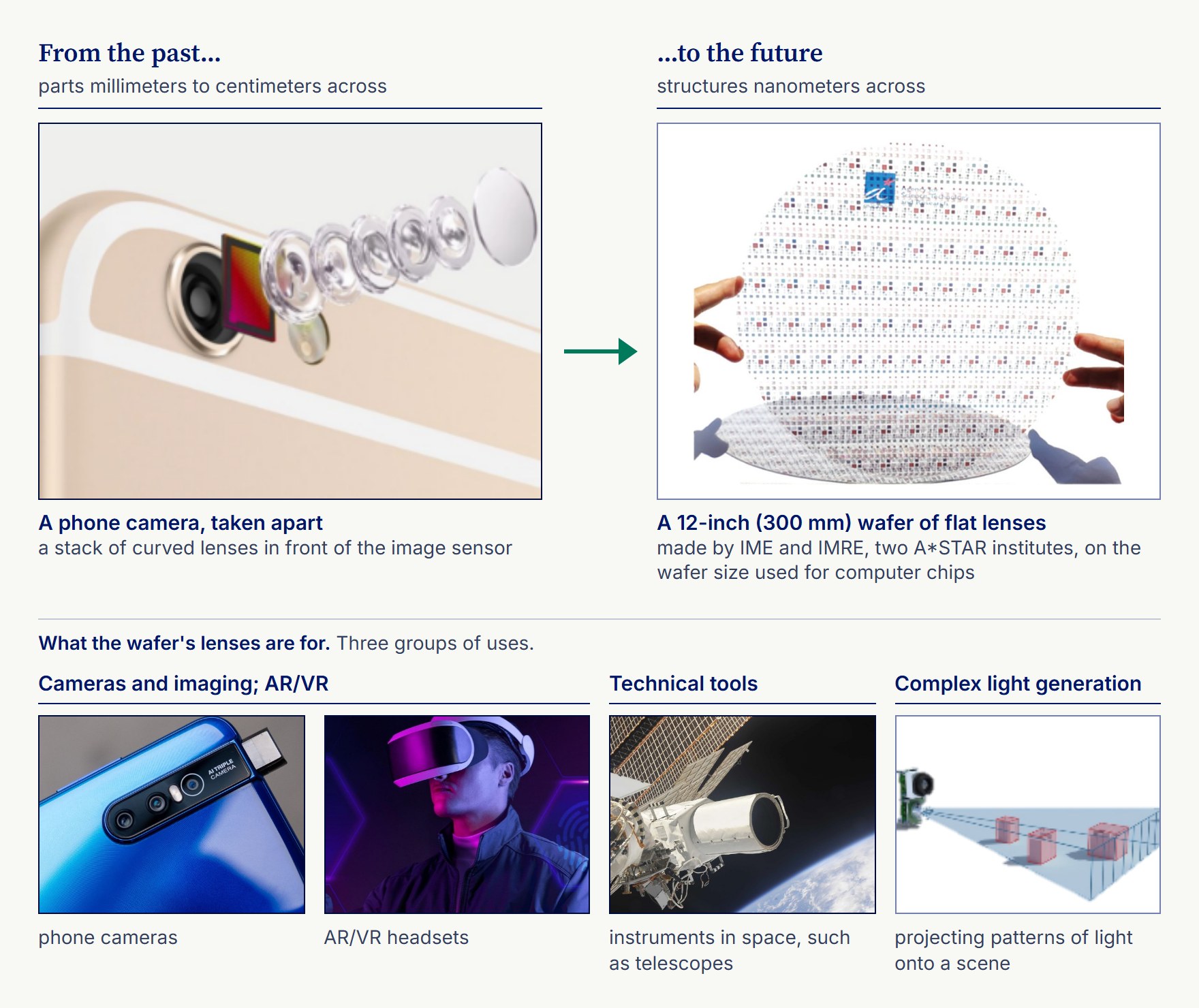
A curved lens has to be thick to bend light strongly, and a single lens blurs colors and edges, so a phone camera stacks several lens elements, each one made and lined up with care. That stack is the bump on the back of every phone. The other parts inside the phone have shrunk year after year; the lens has barely changed its principle in four centuries.
Muốn bẻ ánh sáng thật mạnh, thấu kính cong phải dày, mà một thấu kính đơn lẻ lại làm nhòe màu sắc lẫn đường viền. Vì thế camera điện thoại phải xếp chồng nhiều thấu kính, cái nào cũng chế tạo và căn chỉnh tỉ mỉ. Chồng thấu kính ấy chính là phần lồi ở mặt sau mọi chiếc điện thoại. Các bộ phận khác của điện thoại năm nào cũng nhỏ đi; còn thấu kính thì suốt bốn thế kỷ gần như không đổi nguyên lý.
A flat lens bends light with nanostructures
Thấu kính phẳng bẻ cong ánh sáng bằng cấu trúc nano
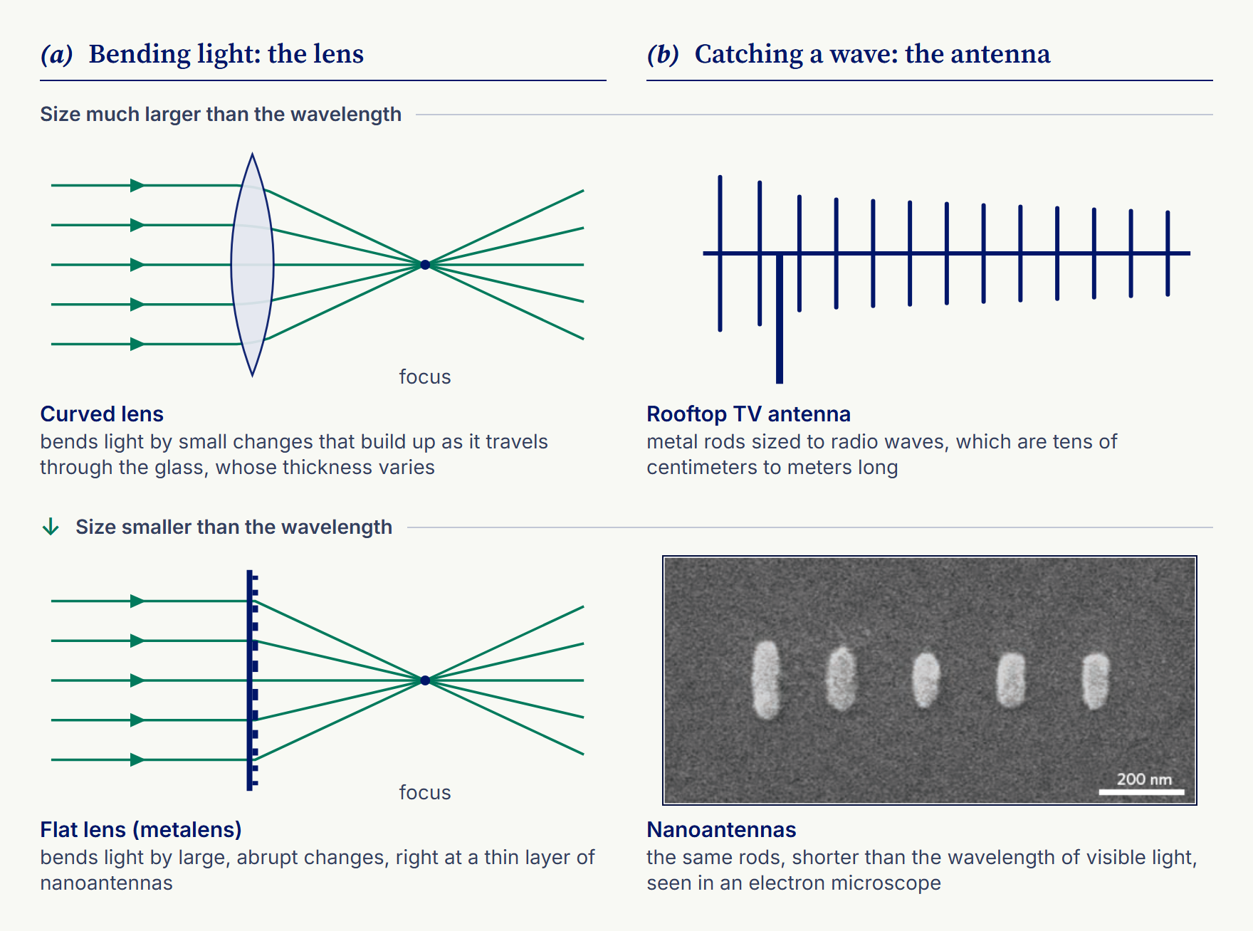
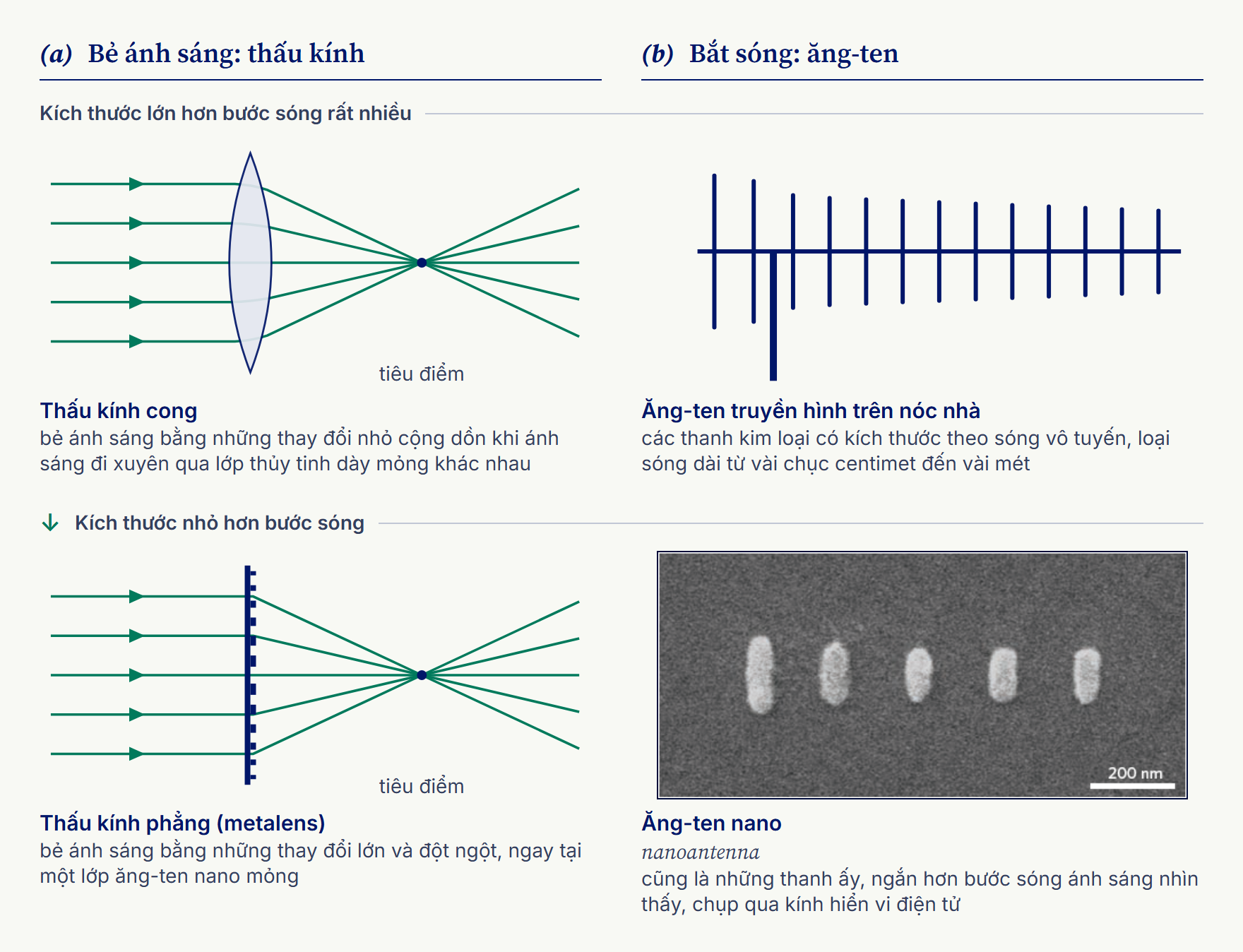
Flat optics bends light another way, with nanostructures built on an idea from radio. Think of the antennas that once stood on every rooftop to catch television signals. Each metal rod is sized to the radio waves it receives, which are tens of centimeters to meters long. Light is a wave too, but visible light has a wavelength of only a few hundred nanometers, and the light in the fibers of chapter 5 about 1.55 micrometers. Shrink the antenna to a few hundred nanometers and it can catch light and send it on: that is a nanoantenna.
Quang học phẳng (flat optics) bẻ cong ánh sáng theo một cách khác: dùng những cấu trúc nano dựa trên một ý tưởng mượn từ kỹ thuật vô tuyến. Hãy nhớ lại những cây ăng-ten từng dựng trên nóc mọi ngôi nhà để bắt sóng truyền hình. Mỗi thanh kim loại có chiều dài tương ứng với sóng vô tuyến mà nó thu, loại sóng dài từ vài chục centimet đến vài mét. Ánh sáng cũng là sóng, nhưng ánh sáng nhìn thấy có bước sóng chỉ vài trăm nanomet, còn ánh sáng trong sợi quang ở chương 5 có bước sóng khoảng 1,55 micromet. Thu nhỏ cây ăng-ten xuống cỡ vài trăm nanomet, nó sẽ bắt được ánh sáng rồi phát đi tiếp: đó là một ăng-ten nano (nanoantenna).
Each of these tiny structures passes the light that reaches it on with a small delay, set by its size and shape; some do it by resonating with the light, a cousin of the effect the ring resonator of chapter 2 uses to pick out one color. Lay out a great many of them across a flat surface, each tuned slightly differently, and the delays add up to the effect a curved lens gets from its changing thickness: the light leaving the layer is steered toward a focus. A patterned layer like this is called a metasurface, and one designed to focus light is a metalens, or flat lens. The contrast is simple: a curved lens bends light by its shape, a flat lens by a pattern of tiny structures.
Mỗi cấu trúc tí hon ấy cho ánh sáng chiếu tới đi qua nhưng làm nó trễ đi một chút, tùy theo kích thước và hình dạng của nó. Một số cấu trúc làm được việc này nhờ cộng hưởng với ánh sáng, một hiệu ứng gần với cách vòng cộng hưởng (ring resonator) ở chương 2 chọn ra một màu ánh sáng. Xếp thật nhiều cấu trúc như vậy trên một mặt phẳng, mỗi cái chỉnh lệch nhau một chút, các độ trễ cộng lại sẽ cho cùng tác dụng mà thấu kính cong có được nhờ độ dày thay đổi: ánh sáng rời khỏi lớp ấy bị lái về một tiêu điểm. Một lớp mang hình mẫu nano như thế gọi là metasurface, và loại thiết kế để hội tụ ánh sáng gọi là metalens, hay thấu kính phẳng. Sự khác biệt rất đơn giản: thấu kính cong bẻ ánh sáng nhờ hình dạng của nó, còn thấu kính phẳng nhờ một hình mẫu gồm những cấu trúc tí hon.
Curved glass lensThấu kính thủy tinh cong plano-convex, n = 1.5phẳng-lồi, n = 1,5
thinnest, at 20 mmmỏng nhất, ở 20 mm
- Centre thicknessĐộ dày ở tâm
- 0.98 mm0,98 mm
- Radius of the curved faceBán kính mặt cong
- 7.0 mm7,0 mm
Metalens a flat layer of nanopillarsmột lớp phẳng gồm các trụ nano (nanopillar)
- ThicknessĐộ dày
- 0.6 µm at every focal length0,6 µm ở mọi tiêu cự
- 2π zones, centre to edgeSố vùng 2π, từ tâm ra mép
- 577
- Zone width at the edgeĐộ rộng vùng ở mép
- 2.6 µm2,6 µm
Metalens pillars, magnifiedCác trụ nano của metalens, phóng to
Halfway out, 1.5 mm from the centreỞ nửa đường, cách tâm 1,5 mm
At the edge, 3 mm from the centreỞ mép, cách tâm 3 mm
Top line: the delay each spot must add, from 0 to one full wave (2π); it resets at each zone edge. Wider pillar, more delay. 9 µm shown, edge to the right.Đường phía trên: độ trễ mà từng điểm phải thêm vào, từ 0 đến một bước sóng trọn vẹn (2π); nó quay về 0 ở mỗi ranh giới vùng. Trụ càng rộng, độ trễ càng lớn. Mỗi dải dài 9 µm, phía mép ở bên phải.
Shown at a 14 mm focal length. Turn on JavaScript to change it.Đang hiển thị ở tiêu cự 14 mm. Bật JavaScript để thay đổi tiêu cự.
Both lenses are 6 mm wide and focus green light (550 nm), drawn to the same scale, except that the metalens layer is drawn thicker than its 0.6 µm and the pillar strips are magnified. Rays use the paraxial approximation.Cả hai thấu kính rộng 6 mm và hội tụ ánh sáng xanh lục (550 nm), vẽ cùng một tỉ lệ, trừ lớp metalens được vẽ dày hơn 0,6 µm thật và các dải trụ nano được phóng to. Đường đi của tia sáng tính theo gần đúng cận trục.
The idea is young. Federico Capasso’s group at Harvard showed the first ultrathin flat lens in 2012, working at telecom wavelengths,9.4 and in 2016 the first metalens that works for visible light.9.5 Capasso was already a known name in the field: in 1994, at Bell Labs, he co-invented the quantum cascade laser, a laser for the mid-infrared that also reaches terahertz frequencies.9.6
Ý tưởng này còn rất mới. Năm 2012, nhóm của Federico Capasso ở Harvard lần đầu trình diễn một thấu kính phẳng siêu mỏng, hoạt động ở bước sóng viễn thông.9.4 Năm 2016, nhóm làm ra metalens đầu tiên cho ánh sáng nhìn thấy.9.5 Trước đó Capasso đã là một tên tuổi trong ngành. Năm 1994, tại Bell Labs, ông cùng các đồng nghiệp phát minh ra quantum cascade laser, loại laser cho vùng hồng ngoại giữa, vươn tới cả dải tần terahertz.9.6
What makes flat lenses exciting for industry is how they are made. A metalens is a pattern of nanostructures on a flat wafer, so it can be made with the same lithography and etching tools that make chips. A*STAR, Singapore’s Agency for Science, Technology and Research, makes metasurfaces on 300 mm (12-inch) wafers, the size used for computer chips, with the immersion lithography of a chip fab.9.7 One wafer carries thousands of lenses, all made at once.9.8 As with the photonic chips of chapter 4, none of this needs the leading-edge node: the structures are sized to the wavelength of light, not to the smallest transistor, though they must be made with tight control.
Điều khiến giới công nghiệp hào hứng với thấu kính phẳng nằm ở cách chế tạo. Metalens là một hình mẫu gồm các cấu trúc nano trên một tấm wafer phẳng, nên có thể làm bằng chính các thiết bị quang khắc và khắc dùng để sản xuất chip. A*STAR (Cơ quan Khoa học, Công nghệ và Nghiên cứu Singapore) chế tạo metasurface trên wafer 300 mm, tức 12 inch, cỡ wafer dùng cho chip máy tính. Họ dùng kỹ thuật quang khắc nhúng (immersion lithography) của nhà máy chip.9.7 Một tấm wafer chứa hàng nghìn thấu kính, tất cả làm xong cùng một lúc.9.8 Cũng như các chip quang tử ở chương 4, việc này không cần đến tiến trình bán dẫn (technology node) tiên tiến nhất. Kích thước các cấu trúc tính theo bước sóng ánh sáng, chứ không theo bóng bán dẫn (transistor) nhỏ nhất, dù vẫn phải chế tạo thật chính xác.
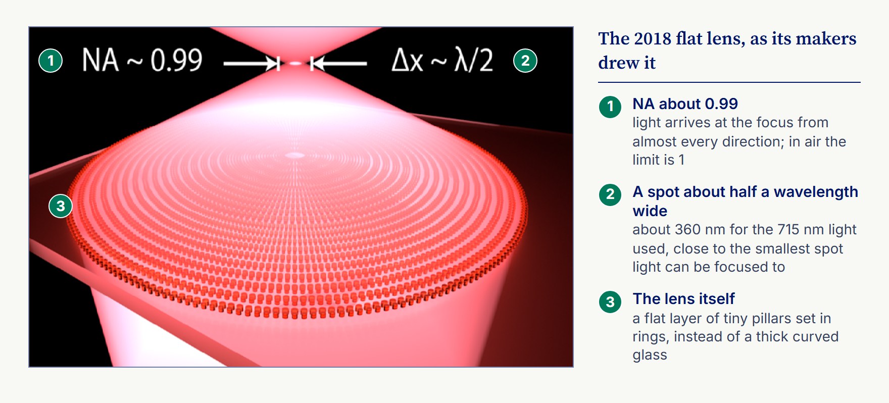
Flat lenses can also do things that are hard for glass. The numerical aperture of a lens measures how wide a cone of light it can gather, and in air it can never exceed 1. In 2018 a team at A*STAR and Nanyang Technological University made a metalens with a numerical aperture of 0.99, beating the previous record of 0.95. Conventional lenses that open that wide are bulky and expensive.9.9
Thấu kính phẳng còn làm được những việc khó với thủy tinh. Khẩu độ số (numerical aperture, NA) cho biết thấu kính gom được một nón ánh sáng rộng đến đâu, và trong không khí, con số này không bao giờ vượt quá 1. Năm 2018, một nhóm nghiên cứu ở A*STAR và Đại học Công nghệ Nanyang (NTU) làm ra một metalens có khẩu độ số 0,99, vượt kỷ lục trước đó là 0,95. Những thấu kính thông thường có độ mở lớn đến thế đều cồng kềnh và đắt tiền.9.9
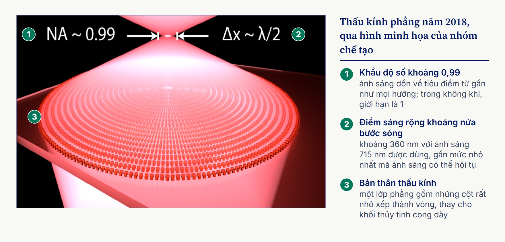
Singapore has built on this work. In 2024 it launched a national center for flat optics and silicon photonics, NSTIC,9.10 and a national R&D fab due to open in 2027 builds on the same platform and will focus first on advanced packaging.9.11 Chapter 10 looks at what Singapore has put into both.
Singapore đã đầu tư tiếp vào hướng nghiên cứu này. Năm 2024, nước này lập trung tâm quốc gia NSTIC cho quang học phẳng và silicon photonics.9.10 Một nhà máy nghiên cứu và phát triển (R&D fab) quốc gia, dự kiến mở cửa năm 2027, sẽ kế thừa nền tảng ấy và trước hết tập trung vào đóng gói tiên tiến (advanced packaging).9.11 Chương 10 sẽ nói rõ Singapore đã đầu tư vào cả hai bao nhiêu.
What flat optics can do next
Quang học phẳng có thể làm gì tiếp theo
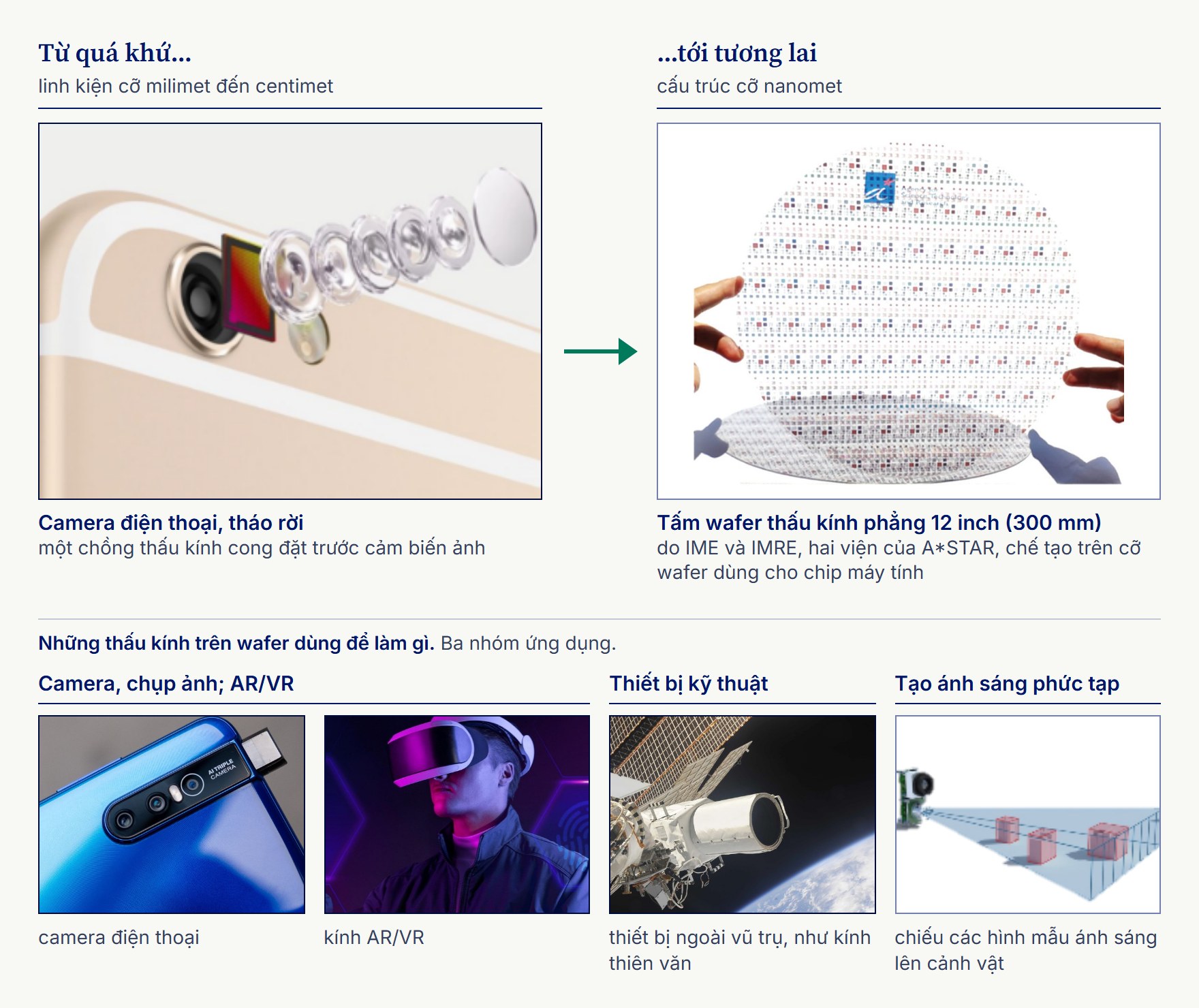
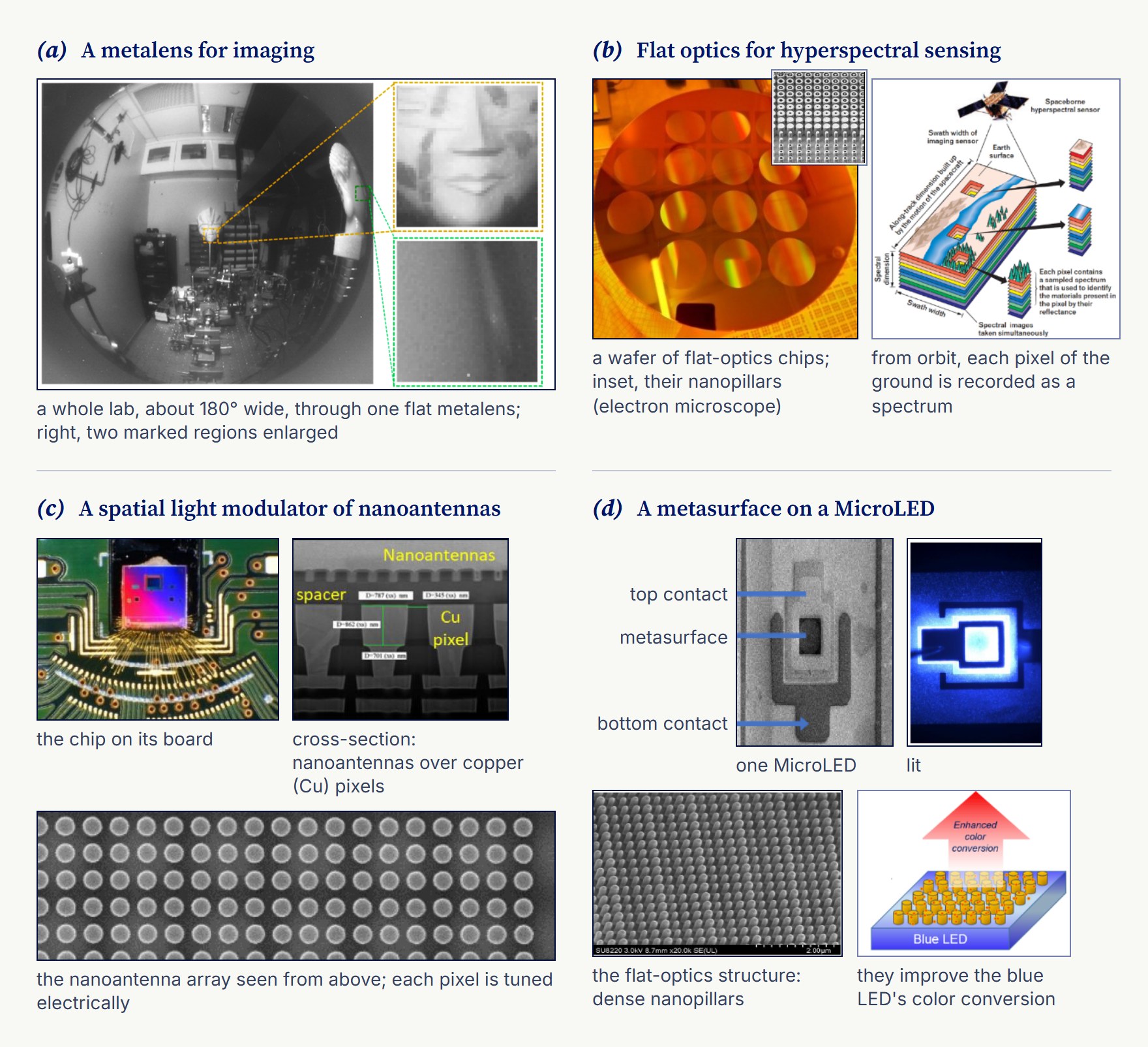
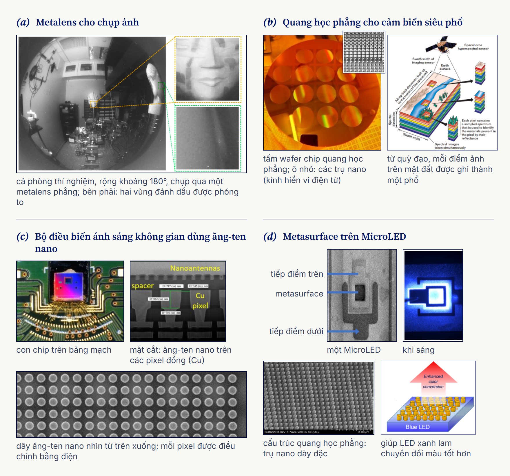
Cameras are only the start. Flat optics has already been shown doing several other jobs, four of them in the plate below.
Camera mới chỉ là bước đầu. Người ta đã thử quang học phẳng cho nhiều việc khác, bốn trong số đó có trong hình dưới đây.
| Use | What the flat optics does | Why it helps |
|---|---|---|
| Wide-angle imaging | One flat lens captures a fisheye view of a whole room | Replaces a thick stack of wide-angle glass |
| Sensing gases from space | Sorts light by wavelength, so each pixel records a spectrum; carbon dioxide and methane each absorb their own bands | Much lighter and smaller than conventional optics, which counts on a satellite9.8 |
| Steering light | A layer of nanoantennas, tuned electrically, bends a beam on command9.12 | Steers light with no moving parts |
| MicroLED displays | Nanostructures on a blue MicroLED improve its color conversion | Brighter full-color pixels for AR glasses |
| Ứng dụng | Quang học phẳng làm gì | Lợi ích |
|---|---|---|
| Chụp ảnh góc rộng | Chỉ một thấu kính phẳng đã thu được ảnh mắt cá (fisheye) của cả căn phòng | Thay cho cả một chồng thấu kính góc rộng dày cộp |
| Đo khí từ vệ tinh | Tách ánh sáng theo bước sóng để mỗi điểm ảnh ghi lại cả một phổ; khí CO₂ và CH₄ hấp thụ ở những dải sóng riêng | Nhẹ và nhỏ hơn hẳn hệ quang học thông thường, điều rất đáng giá trên vệ tinh9.8 |
| Lái chùm sáng | Một lớp ăng-ten nano, điều chỉnh bằng điện, bẻ hướng chùm sáng theo lệnh9.12 | Lái ánh sáng mà không cần bộ phận chuyển động |
| Màn hình MicroLED | Cấu trúc nano phủ trên MicroLED xanh lam giúp chuyển đổi màu tốt hơn | Điểm ảnh đủ màu và sáng hơn cho kính AR |
The next step is to merge flat optics with electronics on one chip, so that a single device both handles electrical signals and shapes light. This is optoelectronics taken down to the nanoscale, and a 2024 review in Science calls such chips optoelectronic metadevices.9.13 A roadmap written the same year by researchers across the field sets out what is still to be solved, from new materials to mass manufacturing.9.14
Bước tiếp theo là hợp nhất quang học phẳng với điện tử trên cùng một con chip, để một linh kiện vừa xử lý tín hiệu điện vừa định hình ánh sáng. Đó là quang điện tử ở cấp độ nano. Một bài tổng quan năm 2024 trên tạp chí Science gọi những con chip như vậy là metadevice quang điện tử.9.13 Cũng trong năm ấy, các nhà nghiên cứu khắp ngành cùng viết một bản lộ trình, liệt kê những việc còn phải giải quyết, từ vật liệu mới đến sản xuất hàng loạt.9.14
Two more uses lie further out and beyond this book: health sensors, such as the imagined blood-sugar watch of chapter 3, and quantum technology, including photonic chips that may one day help build a quantum computer.
Còn hai hướng ứng dụng xa hơn, nằm ngoài phạm vi cuốn sách này: cảm biến sức khỏe, như chiếc đồng hồ đo đường huyết giả định ở chương 3, và công nghệ lượng tử, trong đó có những con chip quang tử một ngày nào đó có thể góp phần làm nên máy tính lượng tử.
When a lens becomes flat and thin, does it lose anything, for example in how much light gets through?Khi thấu kính trở nên phẳng và mỏng, nó có mất gì không, chẳng hạn lượng ánh sáng đi qua có ít đi không?
For a flat lens built for one narrow band of colors, brightness is not the main problem: it can pass light very efficiently, though efficiency still falls in the designs that open widest. Its real drawback is how narrow that band is. Because its tiny structures are designed for particular wavelengths, a flat lens works over only a few tens of nanometers, while a phone camera has to capture everything from blue to red. Covering the whole visible band means stacking several flat lenses, which adds complexity.
Với thấu kính phẳng thiết kế cho một dải màu hẹp, độ sáng không phải vấn đề chính. Loại thấu kính này có thể cho ánh sáng đi qua với hiệu suất rất cao, dù hiệu suất vẫn giảm ở những thiết kế có độ mở lớn nhất. Nhược điểm thật sự của nó là dải bước sóng hoạt động hẹp. Vì các cấu trúc tí hon được thiết kế cho những bước sóng nhất định, thấu kính phẳng chỉ làm việc trong một dải rộng vài chục nanomet, trong khi camera điện thoại phải thu mọi màu từ xanh lam đến đỏ. Muốn phủ hết dải ánh sáng nhìn thấy thì phải xếp chồng vài thấu kính phẳng, và hệ thống sẽ phức tạp hơn.
Where one color is enough, the drawback disappears. Face recognition, for example, works with a single band of near-infrared light and needs no color at all. Metalenses for near-infrared light have already been made on 12-inch wafers,9.7 and since 2022 more than 140 million have shipped in consumer devices, inside sensors that measure distance by time of flight.9.15 Color photography, where no shade may be lost, is the hardest case, and it is the one flat lenses still have to win before they reach every phone camera.
Với những ứng dụng chỉ cần một màu, nhược điểm ấy biến mất. Chẳng hạn, nhận diện khuôn mặt chỉ dùng một dải ánh sáng hồng ngoại gần và hoàn toàn không cần màu sắc. Metalens cho ánh sáng hồng ngoại gần đã được chế tạo trên wafer 12 inch,9.7 và từ năm 2022 đã có hơn 140 triệu chiếc nằm trong các thiết bị tiêu dùng, bên trong những cảm biến đo khoảng cách bằng thời gian bay.9.15 Chụp ảnh màu, vốn không được để mất một sắc độ nào, là trường hợp khó nhất. Thấu kính phẳng còn phải vượt qua nó thì mới có mặt trên mọi camera điện thoại.
Flat optics is still a research field, so a practical way in runs through research labs. Singapore’s NSTIC invites university staff and students to work with it, and A*STAR offers scholarships from undergraduate to postdoctoral level, with attachments even for pre-university students.9.16 Singapore is a short flight from Vietnam. A few months as an intern in a working clean room is a common first step, and a student who finds the work suits them can go on to a master’s or a PhD in the field.
Quang học phẳng vẫn là một lĩnh vực nghiên cứu, nên một con đường thiết thực để vào ngành là bắt đầu từ các phòng thí nghiệm nghiên cứu. NSTIC của Singapore mời giảng viên và sinh viên đại học đến làm việc cùng. A*STAR có học bổng từ bậc đại học đến sau tiến sĩ, và cả chương trình thực tập cho học sinh dự bị đại học.9.16 Từ Việt Nam sang Singapore chỉ mất một chuyến bay ngắn. Vài tháng thực tập trong một phòng sạch đang vận hành thường là bước đầu tiên, và sinh viên nào thấy hợp có thể học tiếp lên thạc sĩ hoặc tiến sĩ trong ngành này.