Chapter 3 of 10Chương 3/10 7 min7 phút
Designing a chip for an imagined blood-sugar watchThiết kế chip cho một đồng hồ đo đường huyết giả định
Every chip, electronic or photonic, passes through the same four stages: it is designed, then manufactured, then tested, then packaged into the device it will serve. This chapter stays with the first stage. To make the process easier to picture, it is illustrated with one invented design from start to finish: a watch that measures blood sugar by shining light through the skin. The watch is a thought exercise, not a product.
Con chip nào, dù là chip điện tử hay chip quang tử (photonic integrated circuit), cũng đi qua bốn khâu như nhau: thiết kế, sản xuất, kiểm thử, rồi đóng gói để lắp vào thiết bị sẽ dùng nó. Chương này dừng lại ở khâu đầu tiên. Để bạn có thể hình dung dễ dàng hơn, quy trình sau được minh họa qua một bản thiết kế giả định từ đầu đến cuối: chiếc đồng hồ đo đường huyết bằng cách chiếu ánh sáng xuyên qua da. Chiếc đồng hồ ấy chỉ là một bài tập tư duy, không phải sản phẩm có thật.
In this chapter
Trong chương này
- How a design starts from what the chip must do, not from the chip itself
- Why the choice of light comes before the choice of material
- How single devices are simulated and then joined into a circuit
- What a layout, a GDS file and tape-out are
- Who sits on a photonic-chip design team, and how a student gets there
- Vì sao một bản thiết kế bắt đầu từ việc con chip phải làm gì, chứ không phải từ bản thân con chip
- Vì sao phải chọn ánh sáng trước rồi mới chọn vật liệu
- Từng linh kiện được mô phỏng rồi ghép thành mạch như thế nào
- Layout, file GDS và tape-out là gì
- Ai làm việc trong một nhóm thiết kế chip quang tử, và sinh viên đi đến đó bằng con đường nào
Start from what the chip must do
Bắt đầu từ việc con chip phải làm gì
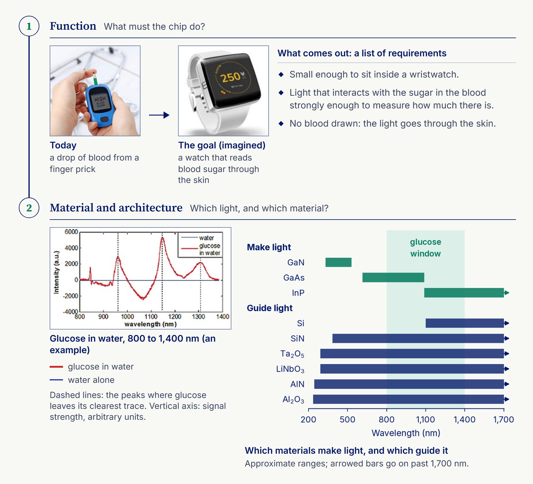
Designing a photonic chip looks much like designing any other chip. It begins with a question that has nothing to do with light: what is the chip for? Here the answer comes from a daily hardship. Many people with diabetes check their blood sugar by pricking a fingertip to draw a drop of blood, often several times a day. A chip that could send light through the skin and read the sugar level without drawing blood would spare them that pain. That is the chip’s function, and in photonics it is where every design starts.
Thiết kế một chip quang tử nhìn chung không khác mấy so với thiết kế các loại chip khác. Mọi thứ bắt đầu từ một câu hỏi chẳng liên quan gì đến ánh sáng: con chip dùng để làm gì? Ở đây, câu trả lời đến từ một nỗi khổ hằng ngày. Nhiều người bệnh tiểu đường phải chích đầu ngón tay lấy một giọt máu để thử đường huyết, có khi vài lần mỗi ngày. Một con chip chiếu ánh sáng qua da và đọc ra lượng đường mà không cần lấy máu sẽ giúp họ khỏi cái đau ấy. Đó là chức năng của con chip, và trong quang tử học (photonics), bản thiết kế nào cũng khởi đầu từ đây.
The function then turns into requirements. The chip has to be small enough to sit inside a wristwatch. And its light has to interact with the sugar molecules in the blood strongly enough to measure how much sugar there is. A chip built for that second job is a kind of glucose sensor, glucose being the sugar the body burns.
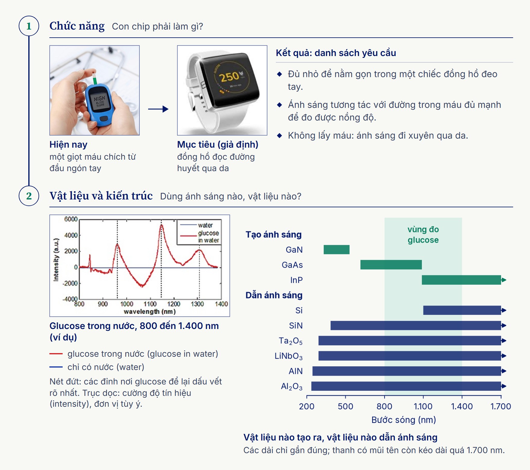
Từ chức năng, người thiết kế rút ra các yêu cầu. Con chip phải đủ nhỏ để nằm gọn trong một chiếc đồng hồ đeo tay. Ánh sáng của nó phải tương tác với các phân tử đường trong máu đủ mạnh để đo được nồng độ. Con chip làm việc thứ hai ấy là một dạng cảm biến glucose (glucose sensor). Glucose chính là loại đường cơ thể dùng làm nhiên liệu.
The goal is real, and it is hard. In 2024 the US Food and Drug Administration warned people not to use smartwatches or smart rings that claim to measure blood sugar without piercing the skin, and stated that it had authorized none of them.3.1 That makes the watch a good exercise: every step below is one a real team would take, and the finished product is still out of reach.
Mục tiêu này có thật, và rất khó. Năm 2024, Cơ quan Quản lý Thực phẩm và Dược phẩm Hoa Kỳ (FDA) khuyến cáo người dân đừng dùng đồng hồ hay nhẫn thông minh tự nhận là đo đường huyết mà không cần chích qua da. Cơ quan này cũng nói rõ họ chưa cấp phép cho thiết bị nào như thế.3.1 Chính vì vậy chiếc đồng hồ là một bài tập hay. Bước nào dưới đây cũng là bước mà một nhóm thiết kế ngoài đời thực phải làm, còn sản phẩm hoàn chỉnh thì vẫn nằm ngoài tầm với.
Pick the light, then the material
Chọn ánh sáng trước, rồi mới chọn vật liệu
The second step asks how glucose behaves in light. Every kind of molecule responds more strongly to some wavelengths than to others, and the pattern it makes across the wavelengths, its spectrum, works like a fingerprint. The plate above includes an example: a spectrum of glucose in water between 800 and 1,400 nm, in the near-infrared just beyond the red end of what eyes can see. The designer looks for the wavelengths where glucose leaves its clearest trace against the water around it, a very small signal, and picks those.
Ở bước thứ hai, người thiết kế tìm hiểu xem glucose ứng xử thế nào trước ánh sáng. Mỗi loại phân tử phản ứng mạnh với bước sóng này hơn bước sóng khác, và cách nó phản ứng trên cả dải bước sóng, tức phổ của nó, giống như một dấu vân tay. Hình minh họa ở trên có kèm một ví dụ: phổ của glucose trong nước, từ 800 đến 1.400 nm, thuộc vùng cận hồng ngoại, ngay ngoài rìa đỏ của vùng ánh sáng mắt người nhìn thấy. Người thiết kế tìm những bước sóng mà ở đó glucose để lại dấu vết rõ nhất so với nước xung quanh, dù tín hiệu ấy rất nhỏ, rồi chọn chúng.
Only then comes the material, because no single material can make and carry every color of light. Some materials are good at giving off light at a certain range of wavelengths, others at guiding it with little loss, and each covers only part of the spectrum. Silicon on its own, for example, limits the wavelengths a chip can use, which is why materials such as silicon nitride are brought in to reach shorter ones.3.2 A second chart in the plate, of materials against wavelength, maps that choice: which material systems make light at which wavelengths, and which can guide it. Chapter 4 looks at those materials one by one.
Đến lúc ấy mới tới chuyện vật liệu, vì không có vật liệu nào vừa tạo ra vừa dẫn được mọi màu ánh sáng. Có vật liệu giỏi phát sáng trong một khoảng bước sóng nhất định, có vật liệu giỏi dẫn sáng mà ít hao hụt, và mỗi loại chỉ phủ một phần của phổ. Chẳng hạn, nếu chỉ có silicon thì con chip bị bó hẹp trong một dải bước sóng. Muốn với tới các bước sóng ngắn hơn, người ta phải đưa thêm những vật liệu như silicon nitride vào.3.2 Một biểu đồ khác trong hình, xếp các vật liệu theo bước sóng, vẽ lại chính lựa chọn đó: hệ vật liệu nào phát sáng ở bước sóng nào, hệ nào dẫn được ánh sáng. Chương 4 sẽ lần lượt xem xét từng loại vật liệu.
What comes out of this step is the chip’s basic architecture: which of the building blocks from chapter 2 it needs, and in what order. For the watch that means a light source at the chosen wavelengths, waveguides to carry the light to the skin and back, and a photodetector to measure what returns.
Kết quả của bước này là kiến trúc cơ bản của con chip: nó cần những khối nào trong số các khối đã gặp ở chương 2, và sắp chúng theo thứ tự nào. Với chiếc đồng hồ, đó là một nguồn sáng ở các bước sóng đã chọn, những ống dẫn sóng (waveguide) đưa ánh sáng tới da rồi dẫn ngược về, và một bộ tách sóng quang (photodetector) để đo phần ánh sáng quay trở lại.
Simulate, then connect the pieces
Mô phỏng từng linh kiện rồi ghép thành mạch
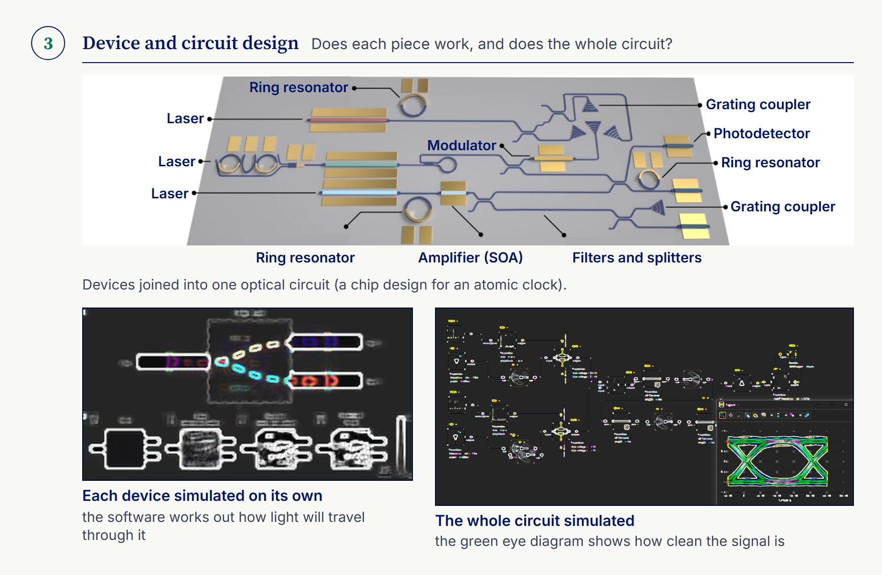
The third step is done almost entirely on a computer. Each device, a waveguide, a splitter, a ring resonator or a modulator, is designed and simulated on its own: the software works out how light will travel through it before anything is made. These devices are the Lego pieces of the chip. Once each piece behaves, the pieces are connected into an optical circuit, and the circuit is simulated as a whole to see whether it does the job the first step asked for.
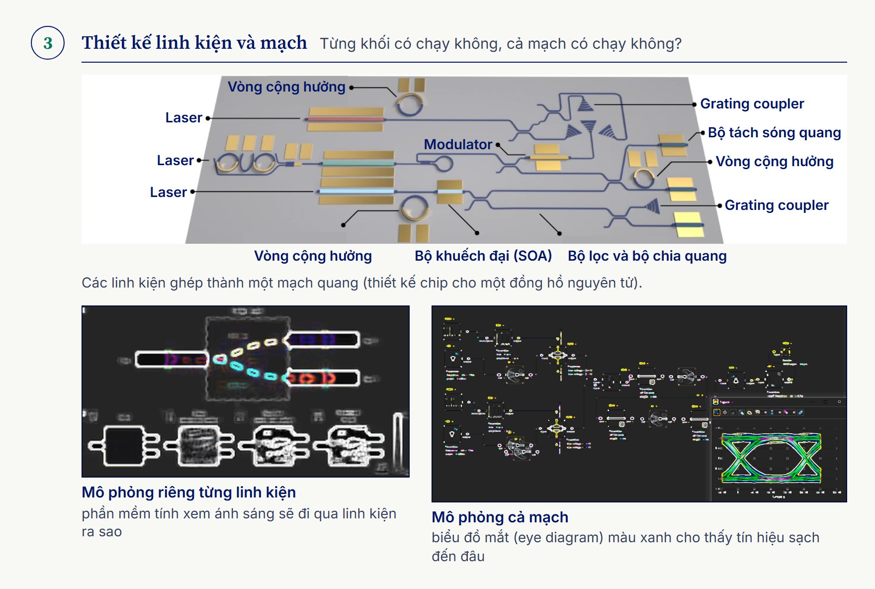
Bước thứ ba gần như diễn ra trọn vẹn trên máy tính. Người thiết kế lần lượt thiết kế và mô phỏng riêng từng linh kiện: ống dẫn sóng, bộ chia quang (splitter), vòng cộng hưởng (ring resonator), modulator (bộ điều biến quang). Phần mềm tính xem ánh sáng sẽ đi qua linh kiện ra sao, trước khi có bất cứ thứ gì được chế tạo. Các linh kiện ấy là những mảnh Lego của con chip. Khi từng mảnh đã chạy đúng, người ta ghép chúng thành một mạch quang và mô phỏng cả mạch, xem nó có làm đúng việc mà bước đầu tiên đặt ra hay không.
The plate below shows both levels: simulations of single devices, a circuit that joins ring resonators, a modulator and an optical amplifier, and a circuit being simulated, with the green eye diagram engineers use to judge how clean a signal is.
Hình minh họa dưới đây cho thấy cả hai cấp độ: mô phỏng từng linh kiện riêng lẻ, một mạch nối các vòng cộng hưởng, một modulator và một bộ khuếch đại quang, rồi một mạch đang chạy mô phỏng, kèm biểu đồ mắt (eye diagram) màu xanh mà kỹ sư dùng để xem tín hiệu sạch đến đâu.
Designers rarely draw every piece from nothing. A factory that makes photonic chips usually offers a process design kit (PDK): a library of building blocks already proven on its own production line, together with the rules for drawing on that line. A design built mostly from PDK blocks has a far better chance of working the first time it is made.3.3
Người thiết kế hiếm khi phải tự vẽ mọi linh kiện từ con số không. Nhà máy làm chip quang tử thường cung cấp một Process Design Kit (PDK), tức bộ thiết kế theo quy trình của nhà máy: thư viện những khối đã được kiểm chứng trên chính dây chuyền của họ, kèm theo các quy tắc phải tuân thủ khi vẽ cho dây chuyền ấy. Bản thiết kế dựng chủ yếu từ các khối có sẵn trong PDK thì khả năng chạy được ngay từ lần chế tạo đầu tiên cao hơn nhiều.3.3
Draw the layout, then check it before tape-out
Vẽ layout, rồi kiểm tra trước khi tape-out
A simulated circuit is still only an idea. The fourth step turns it into a layout: the exact shapes that will be printed onto the wafer, layer by layer, drawn to the nanometer. Layouts are saved in GDS, the standard file format for chip drawings. The layout in the plate below is one, packed with many devices and small chips side by side.
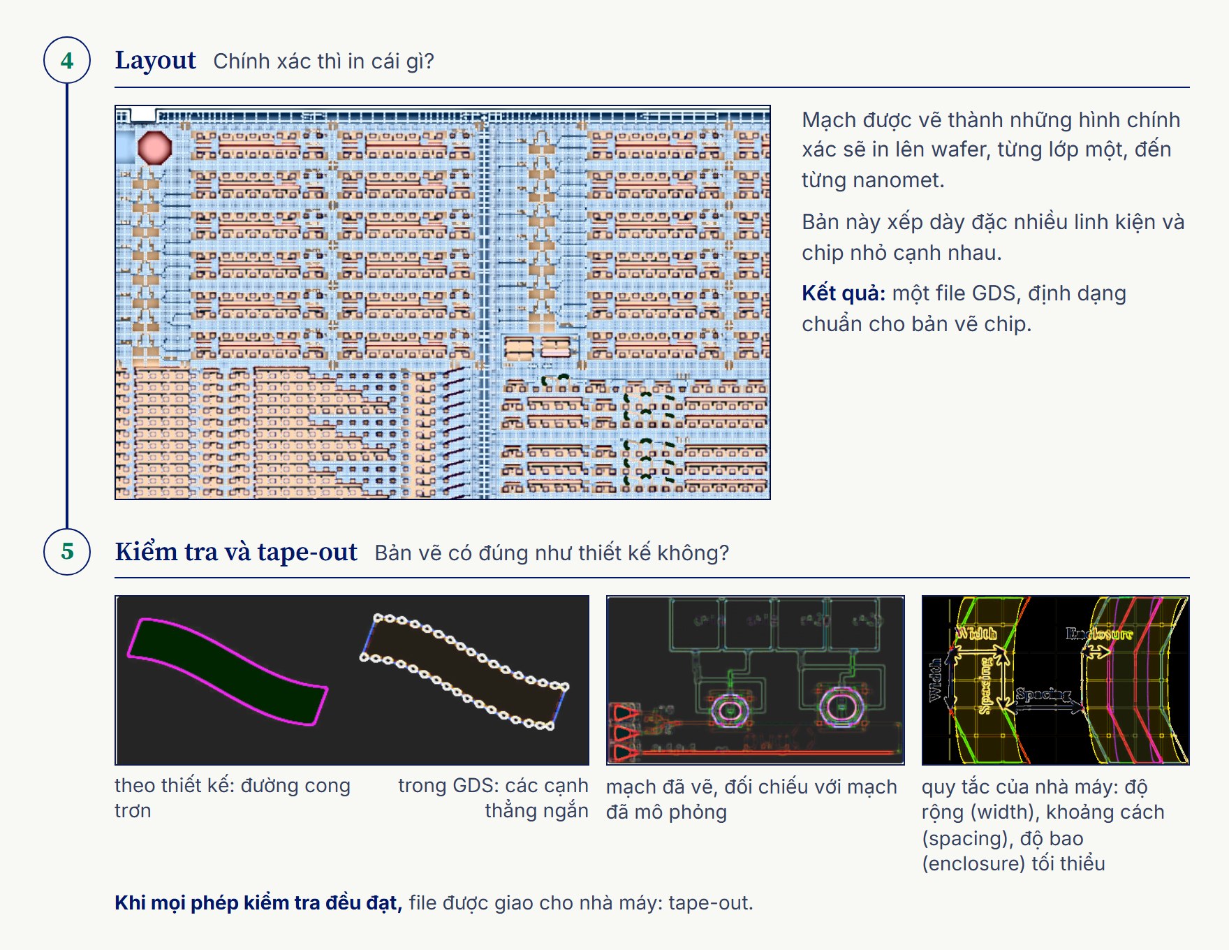
Một mạch đã mô phỏng xong vẫn mới chỉ là ý tưởng. Bước thứ tư biến nó thành layout: những hình vẽ chính xác sẽ in lên wafer, từng lớp một, vẽ đến từng nanomet. Layout được lưu dưới định dạng GDS, loại file chuẩn cho bản vẽ chip. Bản layout trong hình minh họa dưới đây là một ví dụ, dày đặc linh kiện và nhiều con chip nhỏ đặt cạnh nhau.
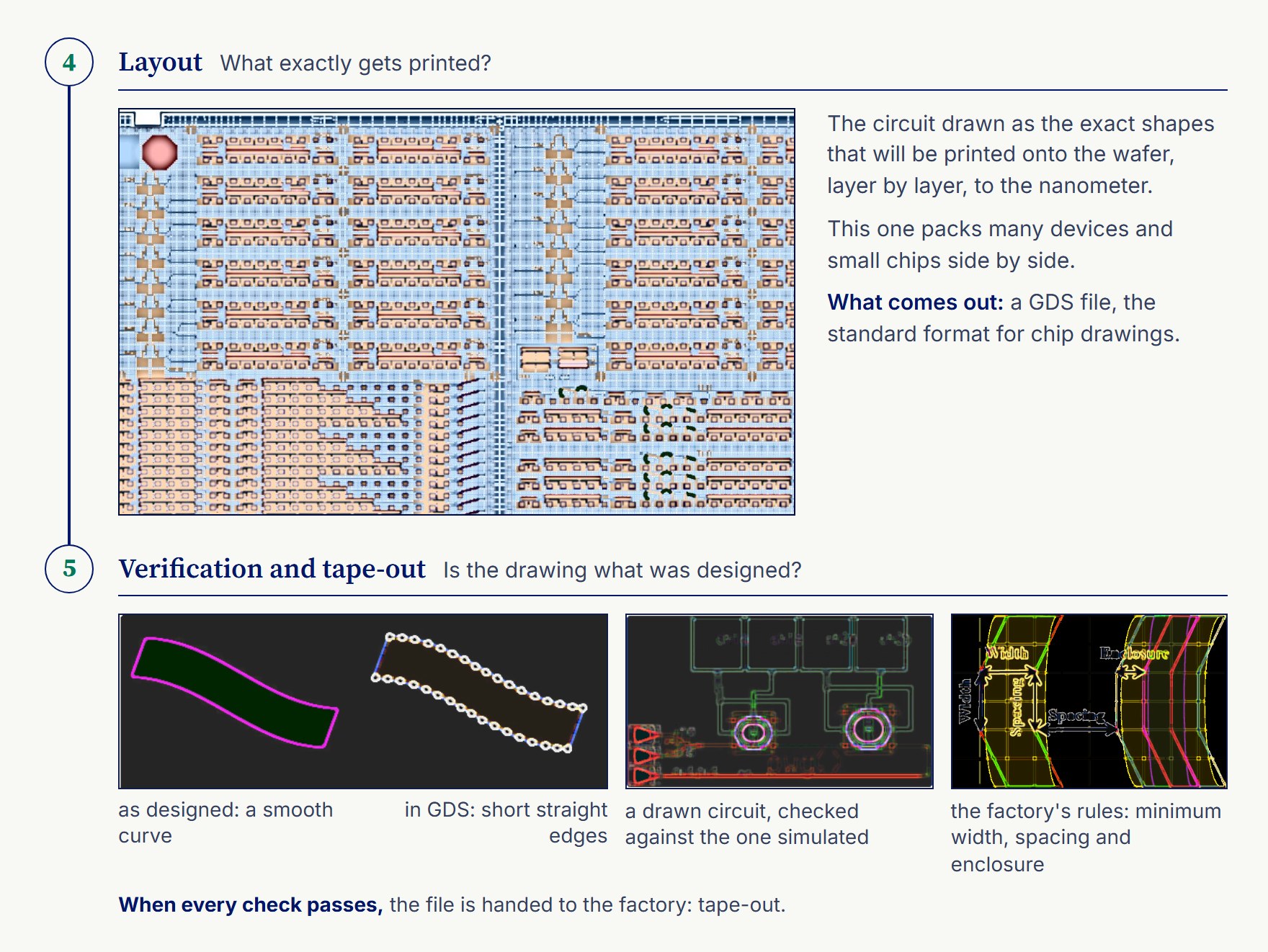
The fifth step is checking. Before anything is sent to be made, the drawing is verified: do the shapes obey the factory’s rules, and is the circuit in the file really the one that was designed and simulated? The first pair of shapes in step 5 of the plate above, a curve as designed beside the same curve in GDS, hints at why this matters for light. A smooth curved waveguide as designed is stored in the GDS file as a chain of short straight edges, and the two must match closely enough that the light cannot tell the difference. When every check passes, the file is handed to the factory. That hand-over is called tape-out.3.3
Bước thứ năm là kiểm tra. Trước khi gửi đi chế tạo, bản vẽ phải qua khâu kiểm định: các hình vẽ có tuân thủ quy tắc của nhà máy không, và mạch trong file có đúng là mạch đã thiết kế và mô phỏng không? Cặp hình đầu tiên ở bước 5 trong hình minh họa phía trên, một đường cong như bản thiết kế đặt cạnh chính đường cong ấy trong GDS, gợi ý vì sao khâu này quan trọng với ánh sáng. Một ống dẫn sóng cong trơn trong bản thiết kế, khi vào file GDS, trở thành một chuỗi cạnh thẳng ngắn nối nhau, và hai hình phải khớp đến mức ánh sáng không phân biệt được. Khi mọi phép kiểm tra đều đạt, file được giao cho nhà máy. Thời điểm bàn giao ấy gọi là tape-out.3.3
The five steps, side by side:
Năm bước ấy, tóm lại trong một bảng:
| Step | The question it answers | In the watch example | What comes out |
|---|---|---|---|
| 1. Function | What must the chip do? | Read blood sugar through the skin, from inside a watch | A list of requirements |
| 2. Material and architecture | Which light, and which material? | The wavelengths where glucose leaves its clearest trace, and materials that make and guide them | The chip’s basic architecture |
| 3. Device and circuit design | Does each piece work, and does the whole circuit? | Light source, waveguides and detector simulated, then joined | A simulated optical circuit |
| 4. Layout | What exactly gets printed? | The circuit drawn as shapes, layer by layer | A GDS file |
| 5. Verification and tape-out | Is the drawing what was designed? | The file checked against the factory’s rules and the simulation | The file sent to the factory |
| Bước | Câu hỏi cần trả lời | Với chiếc đồng hồ | Kết quả |
|---|---|---|---|
| 1. Chức năng | Con chip phải làm gì? | Đọc đường huyết qua da, từ bên trong một chiếc đồng hồ | Danh sách yêu cầu |
| 2. Vật liệu và kiến trúc | Dùng ánh sáng nào, vật liệu nào? | Những bước sóng mà glucose để lại dấu vết rõ nhất, và vật liệu tạo ra, dẫn được chúng | Kiến trúc cơ bản của con chip |
| 3. Thiết kế linh kiện và mạch | Từng khối có chạy không, cả mạch có chạy không? | Mô phỏng nguồn sáng, ống dẫn sóng, bộ tách sóng quang rồi ghép lại | Một mạch quang đã mô phỏng |
| 4. Layout | Chính xác thì in cái gì? | Vẽ mạch thành các hình phẳng, từng lớp một | Một file GDS |
| 5. Kiểm tra và tape-out | Bản vẽ có đúng như thiết kế không? | Đối chiếu file với quy tắc của nhà máy và với kết quả mô phỏng | File gửi sang nhà máy |
A design needs a team from many fields
Một bản thiết kế cần cả một nhóm đến từ nhiều ngành
Those five steps draw on optics, on materials, on electronics and on chip design, which raises a fair question: does one engineer need to know all of it? A doctoral student in the field ends up learning the chain from start to finish. In a company the work is shared. A design team mixes graduates of materials science, chemistry, physics and electrical engineering, and people with very different backgrounds work on the same project to find the solution that best fits what the application needs.
Năm bước ấy cần đến quang học, vật liệu, điện tử lẫn thiết kế chip, nên câu hỏi đặt ra là: một kỹ sư có phải biết hết chừng ấy thứ không? Nghiên cứu sinh trong ngành rốt cuộc sẽ phải học cả chuỗi từ đầu đến cuối. Còn ở công ty thì mỗi người một phần việc. Một nhóm thiết kế quy tụ người tốt nghiệp khoa học vật liệu, hóa học, vật lý và điện, điện tử. Nền tảng mỗi người một khác, nhưng họ cùng làm trong một dự án để tìm ra giải pháp hợp nhất với yêu cầu của ứng dụng.
The person who leads such a design, the chief architect, needs to know enough of each field to bring the specialists together into one chip that works, without mastering every field in depth. Nor does anyone start with all of it. Electrical engineering is a common starting point, and the rest is learned on the job.
Người dẫn dắt một bản thiết kế như thế, tức kiến trúc sư trưởng, cần biết đủ về từng mảng để kết nối các chuyên gia lại, cùng làm ra một con chip chạy được, mà không phải am hiểu sâu mọi lĩnh vực. Cũng chẳng ai có sẵn mọi kiến thức ngay từ đầu. Ngành điện, điện tử là điểm xuất phát thường gặp, phần còn lại học dần trong lúc làm.
For a student the path runs in layers. The foundations, physics and optics, are already taught in the first years of engineering and science degrees. In the third and fourth years, courses on chip architecture can introduce the standard structure of a photonic chip. From there come the new skills this chapter has walked through: simulation, layout, and working from a library of building blocks. Leading a whole design usually takes a master’s degree or a doctorate on top, and each company then trains its new engineers in its own specialties. Courses in photonic-chip design are starting to appear, and the standard textbook on the flow is a good place for any student who wants a head start.3.3
Với sinh viên, con đường này đi từng bậc. Phần nền tảng là vật lý và quang học, vốn đã có trong những năm đầu ở các trường kỹ thuật và khoa học. Lên năm ba, năm tư, các môn về kiến trúc chip có thể giới thiệu cấu trúc tiêu chuẩn của một con chip quang tử. Sau đó mới đến những kỹ năng riêng mà chương này vừa điểm qua: mô phỏng, vẽ layout, làm việc với thư viện các khối có sẵn. Muốn dẫn dắt cả một bản thiết kế thì thường phải học thêm thạc sĩ hoặc tiến sĩ, và công ty nào cũng đào tạo thêm cho kỹ sư mới theo thế mạnh riêng của mình. Các khóa học thiết kế chip quang tử đang dần xuất hiện. Sinh viên nào muốn đi trước một bước cũng có thể tìm đọc giáo trình kinh điển về quy trình này.3.3
Photonic-chip design is within reach of a student with a sound grounding in electrical engineering. The skills that matter first, simulation, layout and working from a building-block library, are learned at a computer, with no factory needed at home, and a finished design can be made abroad, as chapter 10 explains.
Thiết kế chip quang tử nằm trong tầm tay của sinh viên có nền tảng điện, điện tử vững. Những kỹ năng cần trước tiên là mô phỏng, vẽ layout và làm việc với thư viện khối có sẵn. Tất cả đều học bên máy tính, không đòi hỏi trong nước phải có nhà máy. Bản thiết kế hoàn chỉnh có thể gửi ra nước ngoài chế tạo, như chương 10 sẽ trình bày.