Chapter 1 of 10Chương 1/10 9 min9 phút
Chips around usChip ở quanh ta
Pick up almost any electrical device in the room and open it, and you will find a green board dotted with small black squares. Most of those squares are chips. Each chip is an integrated circuit: a crowd of transistors, tiny devices worked by electricity that switch a current on and off or amplify a signal, made together with their wiring on one piece of silicon. Among the largest chips are the GPUs that train AI in data centers, and one of the best known is NVIDIA’s Blackwell.
Cầm lên gần như bất kỳ thiết bị điện nào trong phòng rồi mở ra, bạn sẽ thấy một tấm bo mạch xanh lấm tấm những ô vuông nhỏ màu đen. Phần lớn những ô vuông ấy là chip. Mỗi con chip là một vi mạch: rất nhiều bóng bán dẫn (transistor), những linh kiện tí hon điều khiển bằng điện, có thể đóng ngắt dòng điện hoặc khuếch đại tín hiệu, được chế tạo cùng với dây nối của chúng trên một miếng silicon. Một trong những loại chip lớn nhất là các GPU dùng để huấn luyện AI trong các data center, và trong số đó, Blackwell của NVIDIA thuộc hàng nổi tiếng nhất.
Quick questionThử đoán xem
How many transistors are on NVIDIA's Blackwell chip?Chip Blackwell của NVIDIA có bao nhiêu transistor?
Show the answerXem đáp án
About 200 billion: 208 billion, to be exact, in NVIDIA’s B200, the Blackwell GPU built for data centers. They do not all sit on one piece of silicon. The B200 is built from two dies, two separate pieces of silicon, each close to the largest area, about 26 by 33 mm, that a lithography machine (the machine that prints a chip’s patterns onto silicon with light) can print in one go. The two are joined by a link that carries 10 terabytes a second, so they work as one chip.1.1, 1.2 What a die is, and how one is made, is where this chapter is going.
Khoảng 200 tỷ, chính xác là 208 tỷ, trong B200, GPU Blackwell dành cho data center của NVIDIA. Số transistor ấy không nằm gọn trên một miếng silicon. B200 gồm hai die, tức hai miếng silicon riêng, mỗi miếng gần bằng diện tích lớn nhất, khoảng 26 × 33 mm, mà máy quang khắc (loại máy dùng ánh sáng in hình mẫu của mạch lên silicon) in được trong một lần. Hai die nối với nhau bằng một đường truyền 10 terabyte mỗi giây, nhờ vậy chúng chạy như một con chip duy nhất.1.1, 1.2 Die là gì và người ta làm ra nó như thế nào, chương này sẽ lần lượt kể.
In this chapter
Trong chương này
- Where chips sit in a phone, an AI accelerator card, a mobile base station and an electric car
- Why a chip is usually a part inside a product, not something a shopper buys
- How sand becomes a polished silicon wafer
- How a wafer becomes many dies, and why bigger wafers make cheaper chips
- The three levels at which a die is mounted, and where chip-on-board and advanced packaging fit
- Chip nằm ở đâu trong điện thoại, card accelerator AI, trạm phát sóng di động và ô tô điện
- Vì sao chip thường là linh kiện nằm bên trong sản phẩm, hiếm khi là món hàng người tiêu dùng mua về
- Cát trở thành tấm wafer silicon bóng như gương ra sao
- Một tấm wafer cho ra nhiều die ra sao, và vì sao wafer càng lớn thì chip càng rẻ
- Die được gắn theo ba cấp nào, và chip-on-board cùng đóng gói tiên tiến nằm ở đâu trong đó
Chips are everywhere
Chip có mặt khắp nơi
The phone, the laptop, the television and the air conditioner all have chips inside, and so do cars, factory robots and the probes sent into space. Plate 1.1 opens up four of the places where chips do heavy work.
Điện thoại, máy tính xách tay, ti vi, máy điều hòa, thứ nào bên trong cũng có chip. Ô tô, robot trong nhà xưởng, cả những con tàu thăm dò vũ trụ cũng vậy. Hình 1.1 cho thấy bên trong bốn nơi chip đang gánh những việc nặng.
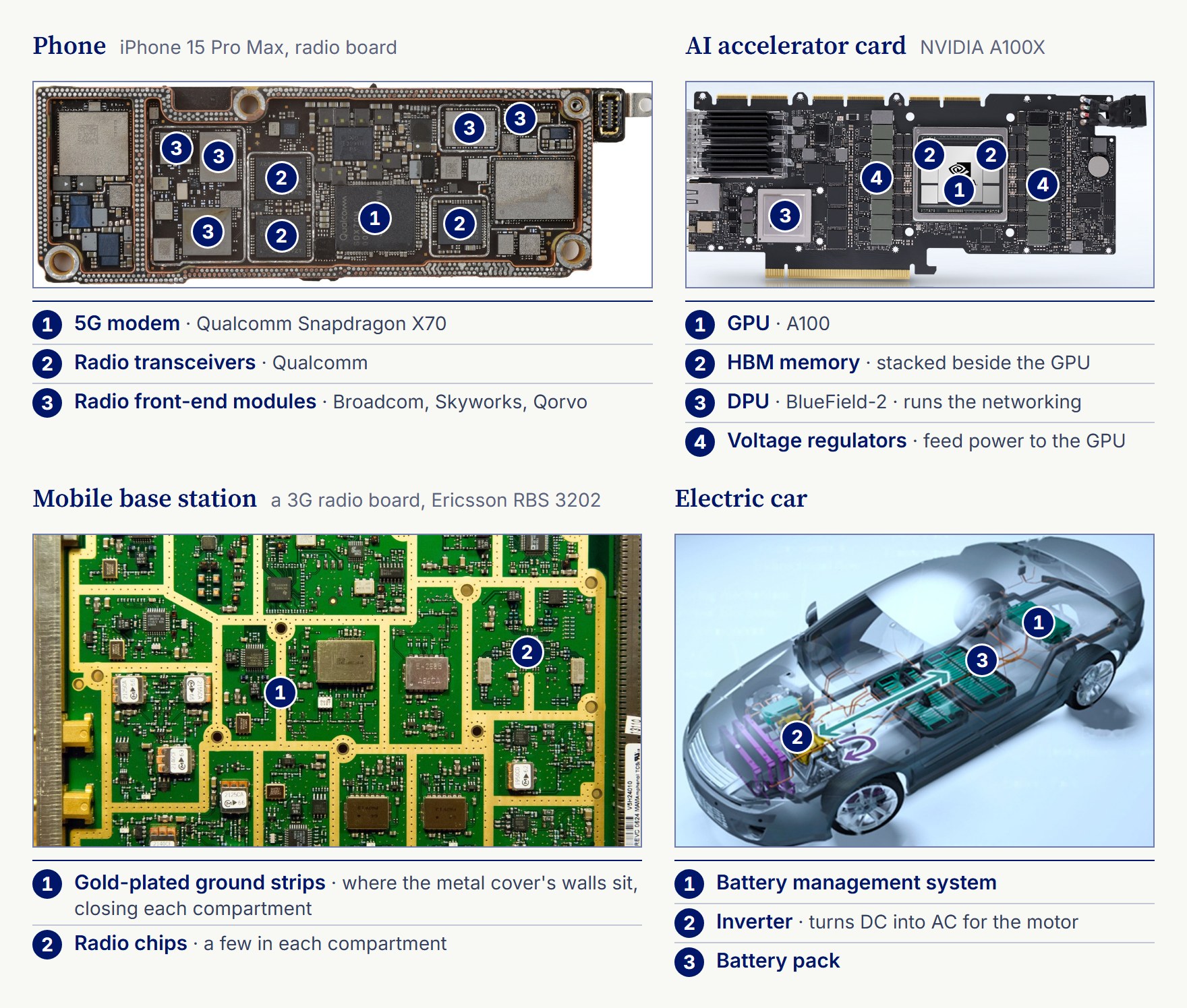
A phone is the chip-packed object nearly everyone carries. The board in plate 1.1 is the radio board of an iPhone 15 Pro Max. It holds a 5G modem, which turns the phone’s data into the signal the mobile network expects and recovers the data from what comes back; transceivers, which shift that signal up to radio frequency and back down; and front-end modules, which amplify and filter the radio signal at the antenna. That one board carries chips from four chip companies: the modem and transceivers come from Qualcomm, the front-end modules from Broadcom, Skyworks and Qorvo.1.3
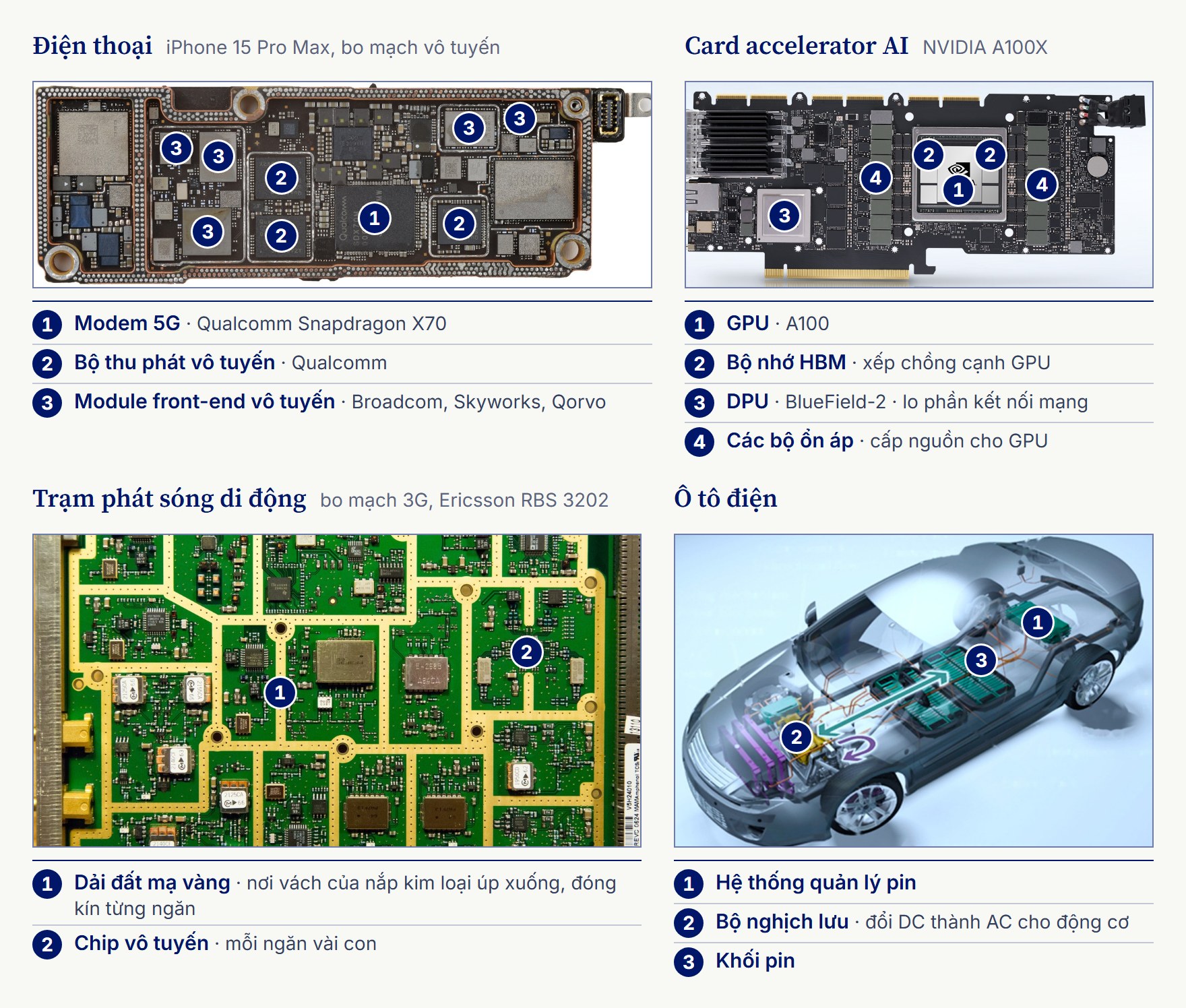
Điện thoại là thứ chứa đầy chip mà hầu như ai cũng mang theo người. Tấm bo trong hình 1.1 là bo mạch vô tuyến của một chiếc iPhone 15 Pro Max. Trên đó có ba loại chip. Modem 5G biến dữ liệu của điện thoại thành tín hiệu theo đúng chuẩn của mạng di động, và lấy lại dữ liệu từ những gì mạng gửi về. Các bộ thu phát nâng tín hiệu ấy lên tần số vô tuyến và hạ xuống ở chiều ngược lại. Các module front-end thì khuếch đại và lọc tín hiệu vô tuyến ở phía ăng-ten. Chỉ riêng tấm bo này đã mang chip của bốn công ty: modem và bộ thu phát của Qualcomm, các module front-end của Broadcom, Skyworks và Qorvo.1.3
In a data center, chips come in much bigger pieces. The card beside the phone board is an NVIDIA A100X accelerator. It has no display output: it is built to run AI and other heavy computing. Right beside the die of its A100 GPU, sealed in the same package, sit stacks of high-bandwidth memory (HBM), 80 GB in all: memory dies piled one on another and joined to the GPU by thousands of short wires side by side, so that data reaches it fast. Elsewhere on the card sit a DPU, a processor of its own that handles the networking, and rows of voltage regulators, which turn the power the card receives into the steady low voltage the GPU needs.1.4, 1.5, 1.6 Chapter 4 follows the design of one such power chip.
Trong data center, chip là những khối lớn hơn nhiều. Tấm card đặt cạnh bo mạch điện thoại là card accelerator NVIDIA A100X. Card này không có cổng xuất hình: nó sinh ra để chạy AI và những phép tính nặng khác. Ngay sát die của GPU A100, trong cùng một package (phần đóng gói của chip), là các chồng bộ nhớ băng thông cao (HBM), tổng cộng 80 GB. Đó là những die nhớ xếp chồng lên nhau, nối với GPU bằng hàng nghìn đường dây ngắn chạy song song, để dữ liệu đến GPU thật nhanh. Ở những chỗ khác trên card có một DPU, bộ xử lý riêng lo phần kết nối mạng. Còn những hàng bộ ổn áp (voltage regulator) biến nguồn điện cấp vào card thành điện áp thấp và ổn định mà GPU cần.1.4, 1.5, 1.6 Chương 4 sẽ theo chân quá trình thiết kế một con chip nguồn như vậy.
A mobile base station, where your phone joins the network, is also a rack of boards full of chips. On the 3G base-station board in plate 1.1, strips of gold-plated copper, joined to the board’s ground, divide it into compartments. A metal cover, taken off for the photo, sits on those strips, so that each stage of the radio is closed in a box of its own and one stage’s signal does not leak into the next.1.7, 1.8 In an electric car, chips manage the battery and drive the motor through the inverter, which turns the battery’s direct current into the alternating current the motor runs on. When the car brakes, the same electronics send power back into the battery.1.9
Trạm phát sóng di động, nơi điện thoại của bạn kết nối vào mạng, cũng là cả một dàn bo mạch đầy chip. Trên bo mạch của trạm phát sóng 3G trong hình 1.1, những dải đồng mạ vàng nối đất chia bo thành từng ngăn. Một nắp kim loại úp lên các dải ấy (trong ảnh, nắp đã tháo ra), khép mỗi tầng vô tuyến vào một hộp riêng để tín hiệu của tầng này không lọt sang tầng kia.1.7, 1.8 Trong ô tô điện, chip quản lý pin và điều khiển động cơ qua bộ nghịch lưu, khối mạch biến dòng điện một chiều của pin thành dòng xoay chiều cho động cơ chạy. Khi xe phanh, cũng chính khối điện tử ấy đưa điện năng nạp ngược về pin.1.9
A chip is a part, not a product
Chip là linh kiện, không phải sản phẩm
A chip is rarely something a shopper buys: it is a component, sold to the engineers who build it into boards and products. It sits on a circuit board, the board sits inside a box, and the box is built into a phone, a household appliance or a machine.
Chip hiếm khi là món hàng người tiêu dùng mua về: đó là một linh kiện, được bán cho những kỹ sư đưa nó vào bo mạch và sản phẩm. Nó nằm trên một tấm bo mạch, tấm bo nằm trong một chiếc hộp, và chiếc hộp ấy lại nằm trong điện thoại, đồ gia dụng hay máy móc.
Many people still take chip design and circuit-board design for the same job. They are different. A board designer picks chips and wires them together on a board; a chip designer works on what is inside one of those small black squares. The needs of the products a chip goes into, and of the engineers who build them, decide what it must do. Chapter 2 starts from there.
Nhiều người vẫn nhầm thiết kế chip với thiết kế bo mạch, tưởng đó là cùng một nghề. Thật ra đây là hai việc khác nhau. Người thiết kế bo mạch chọn các con chip rồi nối chúng lại với nhau trên tấm bo; còn người thiết kế chip lo phần nằm bên trong từng ô vuông đen nhỏ ấy. Chính nhu cầu của những sản phẩm chứa con chip, và của những kỹ sư làm ra sản phẩm ấy, quyết định con chip phải làm được những gì. Chương 2 bắt đầu từ chính chỗ đó.
How sand becomes a wafer
Cát trở thành tấm wafer ra sao
Every one of these chips begins, in a sense, as sand. Sand is mostly silicon dioxide, the same compound as quartz, and silicon is the second most common element in the Earth’s crust after oxygen, more than a quarter of it by weight.1.10, 1.11 The sand costs next to nothing; the purity is what costs.
Theo một nghĩa nào đó, con chip nào cũng bắt đầu từ cát. Cát chủ yếu là silicon dioxide, cùng một chất với thạch anh, và silicon là nguyên tố phổ biến thứ hai trong vỏ Trái Đất, chỉ sau oxy, chiếm hơn một phần tư khối lượng của lớp vỏ.1.10, 1.11 Cát thì gần như chẳng tốn tiền; cái đắt là độ tinh khiết.
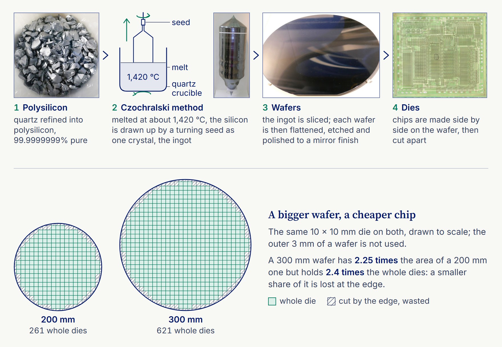
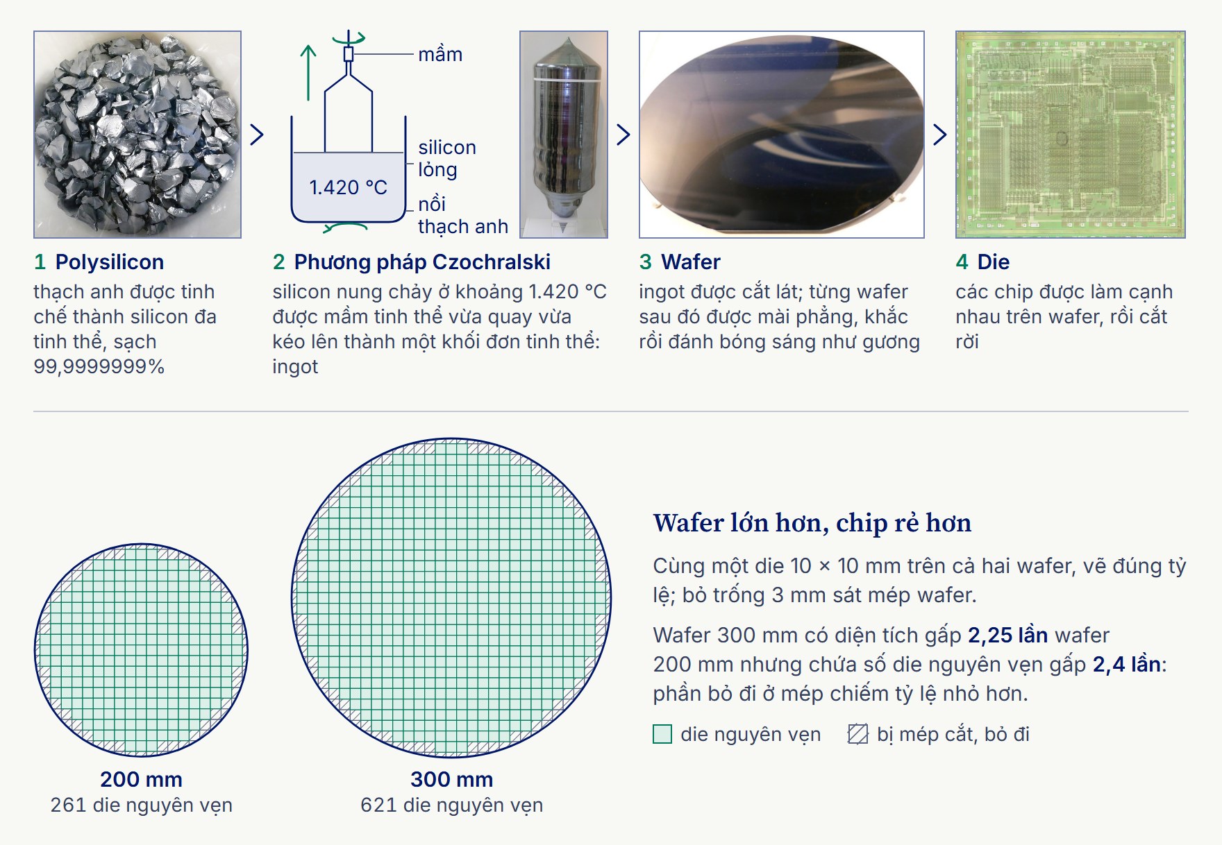
In practice the start is very pure quartz rock, which is first turned into raw silicon, about 98% pure. That silicon is made into a compound that can be purified by distilling it, and the compound is then broken down again, at a high temperature, into solid silicon: polysilicon, so pure that no more than about one atom in a billion is anything else (99.9999999% or better).1.12, 1.13 The polysilicon is melted in a quartz crucible at about 1,420 °C. A small seed crystal is dipped into the melt and drawn slowly upward while it turns, and the silicon freezes onto it as one continuous crystal: a tall, gleaming ingot. This is the Czochralski method.1.14
Trên thực tế, người ta bắt đầu từ đá thạch anh rất sạch và luyện nó thành silicon thô, sạch khoảng 98%. Từ silicon ấy, người ta làm ra một hợp chất có thể tinh lọc bằng chưng cất, rồi phân hủy hợp chất ấy ở nhiệt độ cao để thu lại silicon rắn. Đó là polysilicon, sạch tới mức không quá một nguyên tử lạ trong khoảng một tỷ nguyên tử (độ tinh khiết từ 99,9999999% trở lên).1.12, 1.13 Sau đó, polysilicon được nung chảy trong một nồi thạch anh ở khoảng 1.420 °C. Người ta nhúng một mầm tinh thể nhỏ vào khối silicon lỏng rồi vừa xoay vừa kéo lên thật chậm; silicon đông lại, bám theo mầm thành một khối đơn tinh thể cao và sáng bóng, gọi là ingot. Đó là phương pháp Czochralski.1.14
The ingot is then sliced into thin discs, and each disc is flattened, etched and polished to a mirror finish. That disc is a wafer.1.14 At this point it is a bare wafer, with no circuit on it yet. Bare wafers go to a fab, a chip factory, to have circuits built on them.
Ingot sau đó được cắt thành những lát mỏng; mỗi lát lại qua các bước mài phẳng, khắc và đánh bóng cho tới khi sáng như gương. Lát mỏng ấy chính là wafer.1.14 Lúc này nó mới là wafer trần, chưa có mạch nào. Những tấm wafer trần này sẽ đến nhà máy sản xuất chip (fab), nơi người ta dựng mạch lên chúng.
One wafer yields many dies
Một tấm wafer cho ra nhiều die
Each wafer carries many copies of the same chip side by side: a few dozen of the largest chips, hundreds of a mid-sized one, and thousands of a small chip like the glucose chip of chapter 7. In the fab, the circuits the designers drew are copied onto the wafer one layer at a time. Light prints each layer’s pattern onto a light-sensitive coating, a process called lithography, and that pattern then guides the steps that add material, etch it away or change the silicon. The transistors are made in the silicon at the wafer’s surface, by adding tiny amounts of other elements, dopants; above them come many thin layers of metal wiring, with insulating layers between them, that connect the transistors.
Trên mỗi tấm wafer có nhiều bản sao của cùng một con chip nằm cạnh nhau. Với những con chip lớn nhất, số bản chỉ vài chục; với chip cỡ vừa là hàng trăm; với một con chip nhỏ như chip đo đường huyết ở chương 7 thì lên tới hàng nghìn. Trong fab, mạch điện mà người thiết kế vẽ ra được chép lên wafer theo từng lớp. Ánh sáng “in” hình mẫu của mỗi lớp lên một lớp phủ nhạy sáng, công đoạn gọi là quang khắc; rồi hình mẫu ấy dẫn đường cho các bước phủ thêm vật liệu, khắc bớt đi hoặc biến đổi silicon. Transistor được tạo ngay trong silicon ở bề mặt wafer, bằng cách pha thêm một lượng rất nhỏ nguyên tố khác, gọi là tạp chất. Phía trên là nhiều lớp dây kim loại mỏng, xen giữa là các lớp cách điện, nối các transistor lại với nhau.
When every layer is done, each chip is tested while still on the wafer, and the wafer is cut apart. Each piece is a die: one bare rectangle of silicon holding one copy of the circuit. Die, chip and integrated circuit (IC) name nearly the same thing; “die” is the bare piece, before it is mounted or packaged. The Blackwell GPU of the quiz is made of two of them.
Khi mọi lớp đã xong, người ta kiểm thử từng con chip ngay trên wafer, rồi cắt rời wafer. Mỗi mảnh là một die: một miếng silicon trần hình chữ nhật mang một bản mạch. Die, chip và vi mạch (IC) gần như là một; gọi là die khi nó còn là miếng silicon trần, chưa gắn lên đâu, cũng chưa đóng gói. GPU Blackwell trong câu đố đầu chương gồm hai die như thế.
A bigger wafer holds more dies, yet processing it costs far less than its extra area would suggest. It also loses a smaller share of itself at the edge, where dies are cut off and wasted. Both make each chip cheaper: when the move from 200 mm to 300 mm wafers was announced in 1999, Intel expected it to cut the cost per chip by about 30%.1.15 Plate 1.2 shows the edge effect for one die size: a 300 mm wafer has 2.25 times the area of a 200 mm one, yet holds 2.4 times as many whole dies.
Wafer càng lớn thì càng chứa được nhiều die, trong khi chi phí gia công mỗi tấm tăng chậm hơn nhiều so với phần diện tích tăng thêm. Phần hao hụt ở mép, nơi các die bị cắt dở phải bỏ đi, cũng chiếm tỷ lệ nhỏ hơn. Cả hai điều ấy làm mỗi con chip rẻ đi: khi công bố việc chuyển từ wafer 200 mm sang 300 mm vào năm 1999, Intel dự tính giá thành mỗi con chip sẽ giảm khoảng 30%.1.15 Hình 1.2 cho thấy phần lợi ở mép wafer với một cỡ die cụ thể: diện tích wafer 300 mm gấp 2,25 lần wafer 200 mm, nhưng số die nguyên vẹn lại gấp 2,4 lần.
How a die is mounted
Die được gắn lên bo mạch như thế nào
A bare die is fragile, and its tiny connection pads cannot be soldered onto a board as they are, so it is packaged first. The smallest packages add little more than solder balls on the die itself, as chapter 8 shows. Engineers describe packaging in three levels (plate 1.3). At level 1, the die is sealed in a package, the small black case that protects it and carries its connections out to pins or solder balls: a single-chip package holds one die, a multi-chip package two or more. At level 2, packages are soldered onto a module or card. At level 3, the card plugs into a motherboard, the main board of a computer or server.
Die trần rất dễ hỏng, còn các pad nối tí hon trên đó không hàn thẳng lên bo mạch được, nên trước hết phải đóng gói. Những kiểu đóng gói nhỏ nhất chỉ thêm các viên bi hàn lên chính bề mặt die, như chương 8 sẽ cho thấy. Giới kỹ thuật chia việc đóng gói thành ba cấp (hình 1.3). Ở cấp 1 (level 1), die được bọc kín trong một package, tức khối nhựa nhỏ màu đen vừa bảo vệ die vừa đưa các đường nối của nó ra chân hoặc bi hàn: single chip package chứa một die, còn multi-chip package chứa từ hai die trở lên. Ở cấp 2, các package được hàn lên một module hay card. Ở cấp 3, card cắm vào bo mạch chủ (motherboard), tấm bo chính của máy tính hay máy chủ.
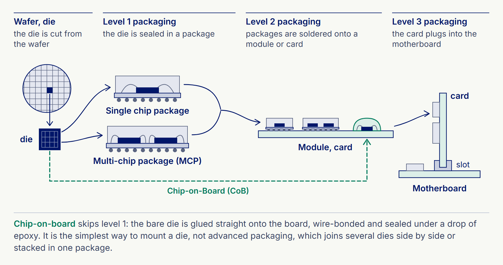
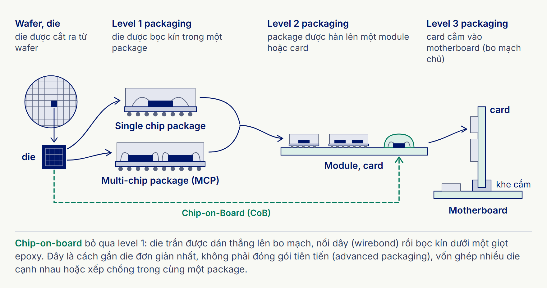
There is a shortcut. Chip-on-board skips level 1: the bare die is glued straight onto the board, wired to it with fine bonding wires and sealed under a drop of epoxy. It is the simplest way to mount a die, and a quick one, which is why chapter 8 shows it used to test a new chip’s first samples.
Cũng có một lối tắt. Chip-on-board bỏ qua cấp 1: die trần được dán thẳng lên bo mạch, nối với bo bằng những sợi dây rất mảnh rồi bọc kín dưới một giọt epoxy. Đây là cách gắn die đơn giản nhất, lại nhanh, nên như chương 8 sẽ cho thấy, người ta dùng nó để thử những mẫu đầu tiên của một con chip mới.
At the other end is advanced packaging, which joins several dies inside one package: side by side on an interposer (2.5D), a thin layer, often of silicon, that carries fine wiring between them, or stacked on top of one another (3D). A processor, its memory and even its power converter then sit millimeters apart.1.16 Blackwell’s two dies, joined into one GPU, are an example, and chapter 4 shows why a power chip is being moved that close to the processor it feeds.
Ở thái cực ngược lại là đóng gói tiên tiến (advanced packaging): ghép nhiều die vào trong cùng một package, hoặc đặt cạnh nhau trên một interposer (2.5D), tức một lớp mỏng, thường bằng silicon, mang dây nối li ti giữa chúng, hoặc xếp chồng lên nhau (3D). Nhờ vậy, bộ xử lý, bộ nhớ, thậm chí cả bộ chuyển đổi nguồn của nó chỉ cách nhau vài milimét.1.16 Hai die của Blackwell ghép lại thành một GPU là một ví dụ. Chương 4 sẽ giải thích vì sao người ta đang đưa chip nguồn lại sát đến thế bên bộ xử lý mà nó cấp điện.