Chapter 3 of 10Chương 3/10 9 min9 phút
Digital design: from code to billions of transistorsThiết kế số: từ dòng code đến hàng tỷ transistor
The NVIDIA Blackwell GPU of chapter 1’s quiz carries 208 billion transistors on two dies, two separate pieces of silicon.3.1 Its designers wrote code, and software did the drawing: it turned the code into gates, the gates into a layout and the layout into the file a foundry needs. This chapter follows that digital design flow, steps 3 to 6 of chapter 2’s map, and the hand-over at tape-out that follows, and shows why a chip of that size takes whole teams of engineers and their tools.
Con chip trong câu đố ở chương 1, GPU Blackwell của NVIDIA, mang 208 tỷ bóng bán dẫn (transistor) trên hai die, tức hai miếng silicon riêng.3.1 Người thiết kế viết code, còn phần vẽ thì phần mềm lo: nó biến code thành cổng logic, cổng logic thành layout, và layout thành tệp mà foundry cần. Chương này đi theo các bước 3 đến 6 của quy trình thiết kế (design flow) trên sơ đồ ở chương 2, phần dành cho thiết kế số (digital design), cùng lần bàn giao tape-out ngay sau đó. Chương cũng cho thấy vì sao một con chip cỡ đó cần tới cả những nhóm kỹ sư cùng công cụ của họ.
In this chapter
Trong chương này
- How chips went from hand drawings to code, and how large they have grown
- What verification checks, and why it takes so many engineers
- How synthesis turns code into standard cells, the building blocks of every digital chip
- How the cells are placed, clocked and wired, and which steps follow
- What power, performance and area mean, and why they pull against each other
- Chip đã chuyển từ bản vẽ tay sang code thế nào, và đã lớn đến đâu
- Kiểm định (verification) kiểm tra những gì, và vì sao cần nhiều kỹ sư đến thế
- Cách tổng hợp logic (synthesis) biến code thành các standard cell, những viên gạch dựng nên mọi con chip digital
- Các cell được xếp chỗ, cấp clock và đi dây thế nào, và những bước nào theo sau
- Công suất, hiệu năng và diện tích là gì, và vì sao chúng giằng co nhau
Before the code, chips were drawn by hand
Trước khi có code, chip được vẽ bằng tay
The first chips were drawn by hand, later on computer screens one shape at a time, and that capped how many circuits one chip could hold. The way past the cap was to describe a circuit in code and let software build the gates. A hardware description language (HDL) reads like a programming language, but what it describes is hardware: which signals exist, and what happens to them on each tick of the clock. The two in wide use are Verilog and VHDL. Verilog now lives on inside a larger language, SystemVerilog, which is built for checking designs as well.3.2 Most digital code is written at the register-transfer level (RTL), which describes how data moves between the chip’s registers on each clock cycle, and what logic sits in between.
Những con chip đầu tiên được vẽ bằng tay, về sau là vẽ trên màn hình máy tính từng hình một, và chính điều đó giới hạn số mạch có thể đặt lên một con chip. Lối thoát là mô tả mạch bằng code rồi để phần mềm dựng các cổng logic. Ngôn ngữ mô tả phần cứng (HDL) trông giống một ngôn ngữ lập trình, nhưng thứ nó mô tả là phần cứng: có những tín hiệu nào, và mỗi nhịp clock thì chúng thay đổi ra sao. Hai ngôn ngữ được dùng rộng rãi là Verilog và VHDL. Verilog nay đã được gộp vào một ngôn ngữ lớn hơn là SystemVerilog, dùng được cả cho việc kiểm tra thiết kế.3.2 Phần lớn code thiết kế digital được viết ở mức RTL (register-transfer level), mô tả dữ liệu di chuyển giữa các register của chip qua từng chu kỳ clock, cùng phần logic nằm giữa chúng.
Turning code into gates is called logic synthesis. It began in research labs and became everyday practice after Synopsys, founded in 1986 to sell synthesis software first built at General Electric, brought out its Design Compiler in the late 1980s.3.3, 3.4 As factories fitted ever more transistors on a chip, these tools kept such chips within their designers’ reach. Today’s biggest GPUs carry a few hundred billion transistors: NVIDIA’s Rubin has 336 billion on two dies (2026). A single chip that takes up most of a silicon wafer carries four trillion transistors (2024).3.5, 3.6
Việc chuyển code thành cổng logic gọi là tổng hợp logic (synthesis). Kỹ thuật này ra đời trong các phòng thí nghiệm nghiên cứu. Nó trở thành cách làm thường ngày sau khi Synopsys, công ty thành lập năm 1986 để bán phần mềm synthesis vốn được làm ra ở General Electric, tung ra Design Compiler vào cuối thập niên 1980.3.3, 3.4 Khi nhà máy đặt được ngày càng nhiều transistor lên một con chip, chính những công cụ ấy giúp người ta vẫn thiết kế nổi các con chip như vậy. Những GPU lớn nhất ngày nay mang vài trăm tỷ transistor: Rubin của NVIDIA có 336 tỷ transistor trên hai die (2026). Một con chip duy nhất chiếm phần lớn diện tích một tấm wafer silicon mang tới bốn nghìn tỷ transistor (2024).3.5, 3.6
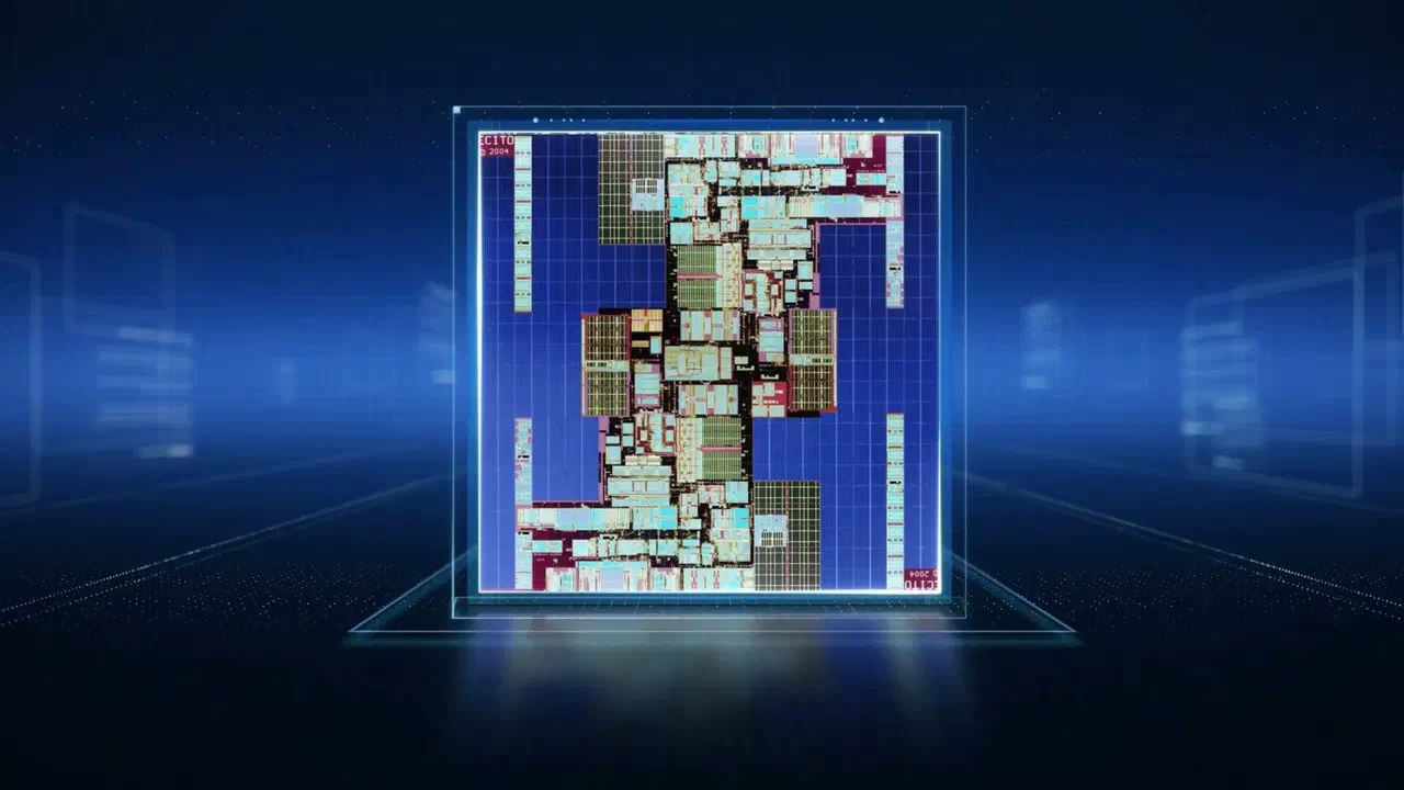
In outline, the digital flow runs in five moves: write the design as RTL, check that it does what it should, turn it into ready-made gates, place and wire those gates, and check the result for timing, power and area before the layout is handed over. The film below follows that journey from the specification to the physical layout; the sections after it take the steps one at a time.
Quy trình thiết kế digital gồm năm chặng: viết thiết kế ở mức RTL, kiểm tra xem nó có làm đúng không, chuyển nó thành các cổng logic làm sẵn, xếp chỗ và đi dây cho các cổng ấy, rồi soát lại timing, công suất và diện tích trước khi bàn giao layout. Đoạn phim dưới đây theo chân hành trình ấy, từ yêu cầu kỹ thuật đến layout vật lý; các phần sau phim đi qua từng bước một.
Checking that the design does what its specification says
Kiểm định xem thiết kế có hoạt động đúng yêu cầu không
Before a single gate exists, the code has to be right. Verification checks that a design does what its specification says. Most of it is functional verification: engineers build a testbench, a program that feeds the design huge numbers of test cases, many of them chosen at random, the unusual ones included, and compares every output with what the specification demands. For a phone’s processor, that means confirming that each function gives the right result before any silicon is made. Some properties of a design are also proved mathematically, with formal methods.
Khi chưa có cổng logic nào, trước hết code phải đúng. Kiểm định (verification) là kiểm tra xem thiết kế có làm đúng như yêu cầu kỹ thuật hay không. Phần lớn việc này là functional verification. Kỹ sư dựng một testbench, tức một chương trình đưa vào thiết kế vô số tình huống thử, phần nhiều chọn ngẫu nhiên, kể cả những ca hiếm gặp. Testbench so từng đầu ra với những gì yêu cầu kỹ thuật đòi hỏi. Với bộ xử lý của điện thoại, điều đó có nghĩa là xác nhận từng chức năng cho kết quả đúng trước khi làm ra bất cứ mẩu silicon nào. Một số tính chất của thiết kế còn được chứng minh bằng toán học, với các phương pháp hình thức (formal methods).
The reason for all this care is cost. A mistake caught in simulation is fixed in the code; the same mistake found in a finished chip means new masks (the stencils that print each layer of the chip) and months of waiting. As chips have grown, verification has claimed more and more of the work. In industry surveys, the average chip project at its busiest now has about as many verification engineers as design engineers, and between 2007 and 2022 the demand for verification engineers grew more than twice as fast as the demand for design engineers.3.7, 3.8
Cẩn thận đến vậy là vì chi phí. Một lỗi bắt được trong mô phỏng thì sửa ngay trong code; cũng lỗi ấy mà lộ ra trên con chip đã làm xong thì phải làm mask mới, tức bộ khuôn để “in” từng lớp chip, rồi chờ thêm nhiều tháng. Khi chip ngày càng lớn, verification cũng chiếm phần việc ngày càng nhiều. Theo các cuộc khảo sát trong ngành, lúc đông người nhất, một dự án chip trung bình ngày nay có số kỹ sư verification xấp xỉ số kỹ sư thiết kế. Từ năm 2007 đến 2022, nhu cầu kỹ sư verification còn tăng nhanh gấp hơn hai lần nhu cầu kỹ sư thiết kế.3.7, 3.8
This is a check of behaviour. The check of the layout, physical verification, comes near the end (step 6 in chapter 2), once there is a layout to check.
Đó là kiểm tra cách hoạt động. Còn kiểm tra layout, tức physical verification, đến gần cuối quy trình (bước 6 ở chương 2), khi đã có layout để soát.
Synthesis turns the code into gates from a standard-cell library
Synthesis chuyển code thành các cổng logic từ thư viện standard cell
Once the code works, synthesis turns it into gates. The synthesis tool reads the RTL and writes a gate-level netlist: a list of logic gates, and of the wires between them, that together do what the code describes.3.9 The gates come ready-made, from a library of standard cells, the building blocks of every digital chip.
Khi code đã chạy đúng, synthesis chuyển nó thành cổng logic. Công cụ synthesis đọc RTL rồi viết ra một gate-level netlist: danh sách các cổng logic và dây nối giữa chúng, cùng nhau làm đúng việc mà code mô tả.3.9 Những cổng ấy được lấy từ một thư viện standard cell làm sẵn, những viên gạch dựng nên mọi con chip digital.
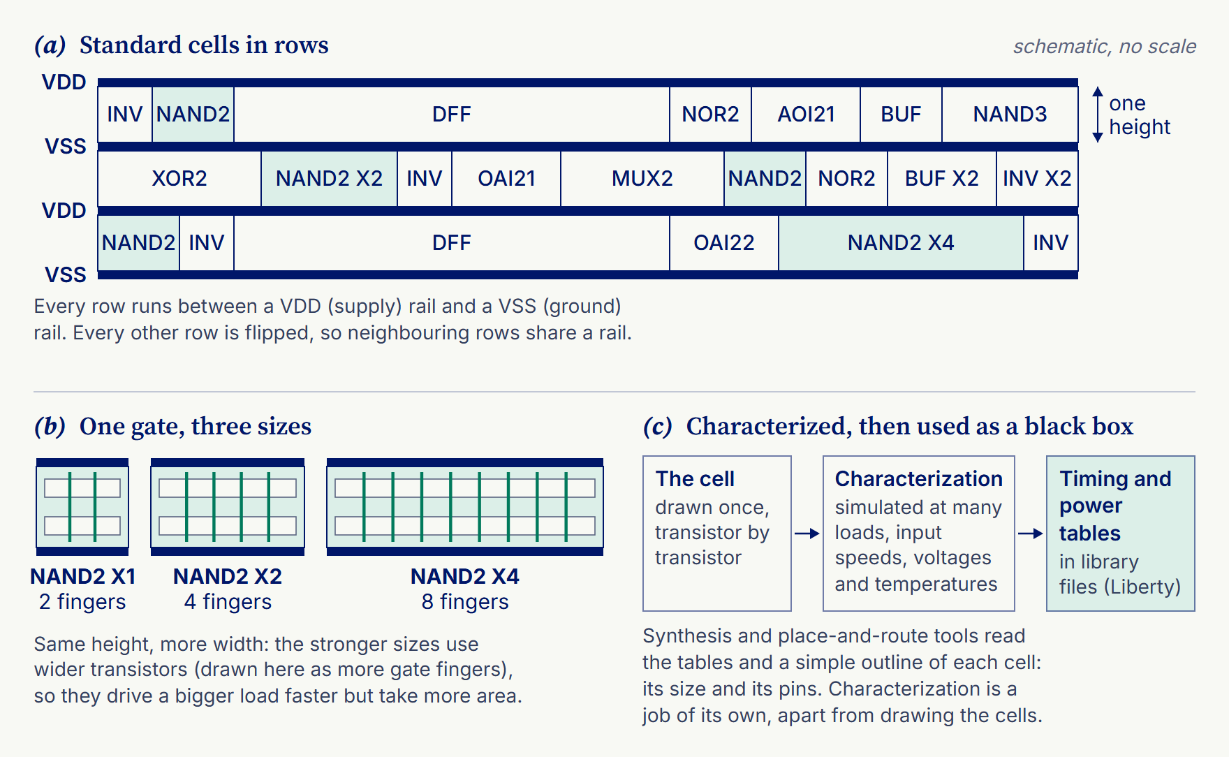
Each standard cell is one small circuit, an inverter, a NAND gate or a flip-flop, drawn once, transistor by transistor. Almost all the cells of a library share one height (a few large ones span two rows), so they line up in rows between shared supply and ground rails, like bricks of one height (plate 3.1a). They differ in width, and each gate comes in several sizes: a larger size uses wider transistors, so it drives a heavier load faster but takes more area (plate 3.1b). The cells, then, share a height, while the transistors inside them vary from cell to cell and from size to size.3.10, 3.11
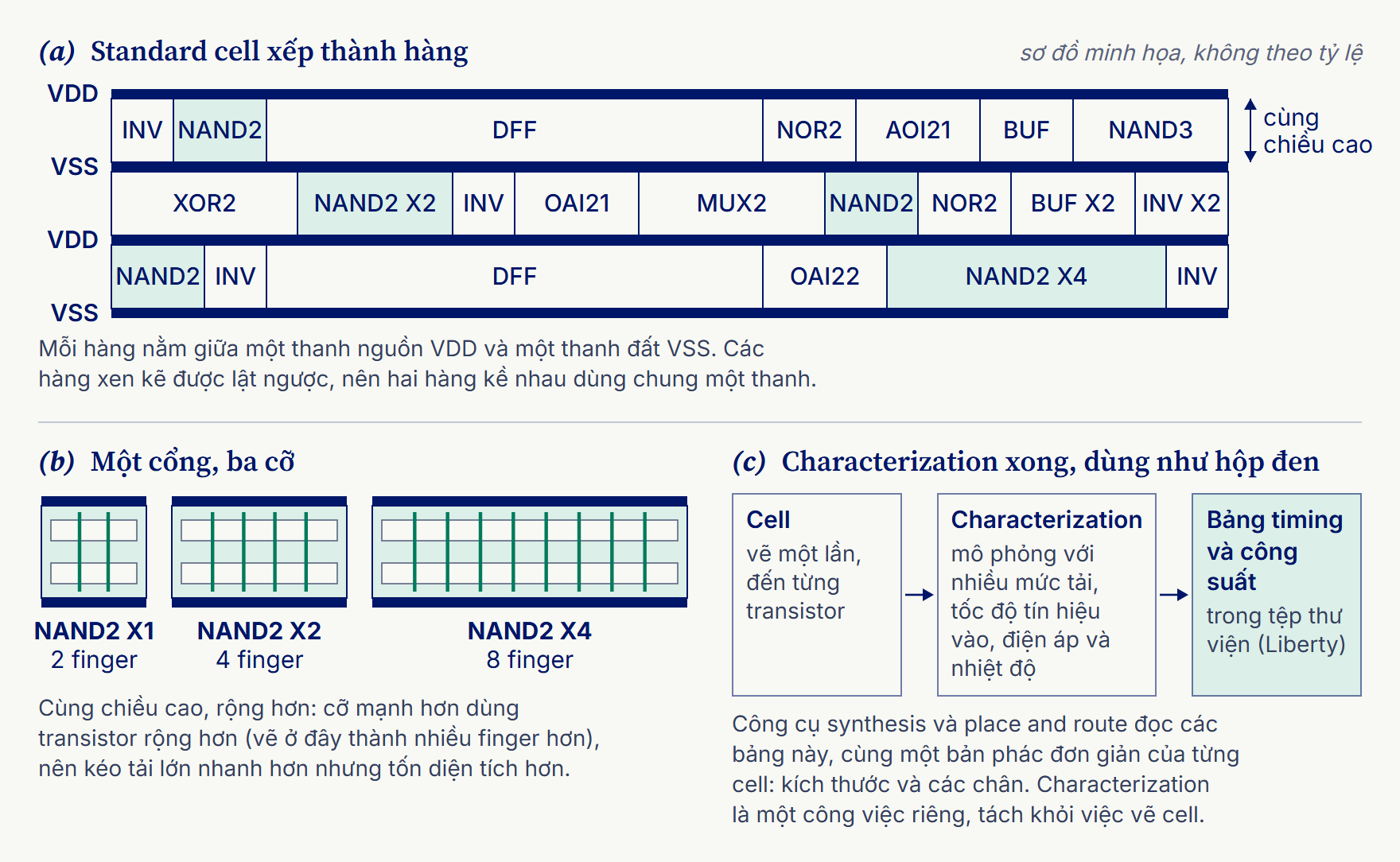
Mỗi standard cell là một mạch nhỏ, như một cổng đảo, một cổng NAND hay một flip-flop, được vẽ sẵn một lần, tới từng transistor. Gần như mọi cell trong một thư viện có cùng chiều cao (một số cell lớn chiếm hai hàng), nên xếp được thành hàng giữa các thanh nguồn và thanh đất dùng chung, như những viên gạch cùng chiều cao (hình 3.1a). Chúng khác nhau ở chiều rộng, và mỗi cổng có nhiều cỡ: cỡ lớn hơn dùng transistor rộng hơn, nên kéo được tải nặng hơn, nhanh hơn, nhưng chiếm nhiều diện tích hơn (hình 3.1b). Vậy các cell có chung chiều cao, còn transistor bên trong thì khác nhau giữa cell này với cell khác, giữa cỡ này với cỡ khác.3.10, 3.11
Before a tool can use a cell, the cell is characterized: simulated at many loads and input speeds, and again at each supply voltage and temperature the chip must work at, and the results stored as tables of its timing and power. Synthesis reads those tables; the layout tools read them too, with a simple outline of each cell that shows only its size and where its pins are. Only the last checks on the finished layout look at the transistors inside (plate 3.1c). Characterizing the cells is a job of its own, apart from drawing them; TSMC, for one, hires engineers for standard-cell characterization alone.3.12
Trước khi công cụ dùng được một cell, cell ấy phải qua characterization: mô phỏng ở nhiều mức tải và nhiều tốc độ tín hiệu vào, lặp lại ở từng mức điện áp nguồn và nhiệt độ mà con chip phải chạy được, rồi lưu kết quả thành bảng timing và công suất. Công cụ synthesis đọc các bảng ấy; công cụ làm layout cũng đọc chúng, kèm một bản phác đơn giản của từng cell, chỉ cho biết kích thước và vị trí các chân. Chỉ những lần kiểm tra cuối cùng trên layout hoàn chỉnh mới nhìn tới transistor bên trong (hình 3.1c). Characterization là một công việc riêng, tách khỏi việc vẽ cell; TSMC chẳng hạn tuyển hẳn kỹ sư chỉ để làm characterization cho standard cell.3.12
This is where digital and analog design part ways. Digital design reaches the transistor too, but mostly through its cells: they are drawn and characterized once, and the tools choose among them. In analog design, the designer, not a tool, chooses the size of every transistor, as the power chip of chapters 4 and 5 shows.
Đây là chỗ thiết kế digital và thiết kế tương tự (analog design) rẽ sang hai hướng. Thiết kế digital cũng chạm tới transistor, nhưng chủ yếu qua các cell: các cell chỉ được vẽ và qua characterization một lần, rồi công cụ chọn trong số đó. Còn ở thiết kế analog, chính người thiết kế, chứ không phải công cụ, chọn kích thước cho từng transistor, như con chip nguồn ở chương 4 và 5 sẽ cho thấy.
Placing and wiring the gates
Xếp chỗ và đi dây cho các cổng logic
A netlist says which gates connect. Where each one sits on the die is the work of place and route, a stage the tool makers call physical implementation, or implementation for short.3.13 It runs through the physical-design steps of chapter 2. Floorplanning arranges the large blocks, placement puts every cell in its row, clock tree synthesis builds the branching network of wires and buffers that brings the clock to every register at nearly the same moment, and routing draws the wires.
Netlist cho biết cổng nào nối với cổng nào. Còn mỗi cổng nằm ở đâu trên die là việc của place and route, công đoạn mà các hãng làm công cụ gọi là physical implementation, hay gọn là implementation.3.13 Công đoạn này đi qua các bước physical design ở chương 2. Floor planning sắp xếp các khối lớn, placement đặt từng cell vào hàng của nó, clock tree synthesis dựng một mạng phân nhánh gồm dây và bộ đệm để clock đến mọi register gần như cùng một lúc, rồi routing đi dây.
The wires run in metal layers stacked above the transistors, joined from one layer to the next by vias; in a layout, each layer has its own colour. A logic chip has about 10 to 15 metal layers, and a leading-edge chip more: Intel’s Intel 4 process has 18.3.14, 3.15 Every shape on every layer must obey the foundry’s design rules, the smallest widths and spacings its process can make.
Dây nối nằm trong các metal layer (lớp dây kim loại) xếp chồng phía trên transistor và được nối từ lớp này sang lớp kế tiếp bằng các via; trong layout, mỗi lớp có một màu riêng. Một con chip logic có khoảng 10 đến 15 metal layer, chip tiên tiến nhất còn nhiều hơn: quy trình Intel 4 của Intel có tới 18.3.14, 3.15 Mọi hình vẽ trên mọi lớp đều phải tuân theo quy tắc thiết kế (design rule) của foundry, tức độ rộng và khoảng cách nhỏ nhất mà quy trình của họ làm được.
The number of ways to do all this is past counting. By Synopsys’s estimate, the ways to place and wire a large chip make a number about 90,000 digits long; the legal positions of Go, a board game known for its vast number of possibilities, make a number 171 digits long.3.16, 3.17 The tools search that space, steered by the goals and limits the engineers set.
Số cách làm tất cả những việc ấy thì không sao đếm xuể. Theo ước tính của Synopsys, số cách xếp chỗ và đi dây cho một con chip lớn là một con số dài khoảng 90.000 chữ số. Còn số thế cờ hợp lệ của cờ vây, trò chơi nổi tiếng vì có quá nhiều khả năng, chỉ là một con số dài 171 chữ số.3.16, 3.17 Công cụ dò tìm trong khoảng không gian ấy, theo những mục tiêu và giới hạn do kỹ sư đặt ra.
Power, performance and area pull against each other
Ba thước đo luôn giằng co: công suất, hiệu năng và diện tích
Every choice along the way is weighed against three measures, known together as PPA: power, the rate at which the chip uses energy; performance, how fast it runs; and area, how much silicon it takes, which sets much of its cost. They pull against each other. A larger cell makes a path faster but costs area and power; a faster clock raises performance and power together. From synthesis to the last check, the engineers’ job is to find the balance the specification asks for.
Mọi lựa chọn trên suốt quy trình đều phải cân theo ba thước đo, gọi chung là PPA (công suất, hiệu năng, diện tích). Công suất là lượng năng lượng con chip tiêu thụ trong mỗi giây; hiệu năng là chip chạy nhanh đến đâu; còn diện tích là con chip chiếm bao nhiêu silicon, thứ quyết định phần lớn giá thành. Ba thước đo này giằng co nhau. Cell cỡ lớn giúp một đường tín hiệu chạy nhanh hơn nhưng tốn diện tích và công suất; clock nhanh hơn thì hiệu năng và công suất cùng tăng. Từ synthesis đến lần kiểm tra cuối cùng, việc của kỹ sư là tìm ra điểm cân bằng mà yêu cầu kỹ thuật đòi hỏi.
Once the architecture is set, performance comes down to timing. Chapter 2’s drawing showed the rule: a signal leaving one register must reach the next before the clock ticks again. It must also not arrive so soon that it spoils what the next register is capturing, a mistake no slower clock can fix. On a large chip both rules are checked on every path, at every supply voltage and temperature the chip is meant for, and the final check, timing signoff, confirms that every signal arrives on time at the target clock speed.
Khi kiến trúc đã định, hiệu năng rốt cuộc là chuyện timing. Hình vẽ ở chương 2 đã cho thấy quy tắc: tín hiệu rời một register phải tới register kế tiếp trước khi clock gõ nhịp tiếp theo. Tín hiệu cũng không được tới quá sớm, làm hỏng dữ liệu mà register kế tiếp đang chốt, một lỗi mà hạ tốc độ clock cũng không sửa được. Trên một con chip lớn, người ta soát cả hai quy tắc ấy trên mọi đường tín hiệu, ở mọi mức điện áp nguồn và nhiệt độ mà con chip phải chạy được. Lần soát cuối cùng, gọi là timing signoff, xác nhận mọi tín hiệu đều đến đúng lúc ở tốc độ clock mục tiêu.
Chapter 4 looks at power from the other side: how that energy reaches the chip. An AI processor draws so much current that the chips that power it have become a design problem of their own.
Chương 4 nhìn công suất từ phía ngược lại: năng lượng ấy đến được với con chip bằng cách nào. Một bộ xử lý AI kéo nhiều dòng điện đến mức những con chip cấp nguồn cho nó đã thành cả một bài toán thiết kế riêng.
From the finished RTL to the file sent to the foundry, the part of the work often called the back end runs through these steps.3.18
Từ bản RTL hoàn chỉnh đến tệp gửi cho foundry, chặng việc thường gọi là back end đi qua các bước sau.3.18
| Step | What happens |
|---|---|
| Turn the code into logic gates (synthesis) | Software turns the RTL code into logic gates and the wires between them |
| Build in ways to test the chip (design for test, DFT) | Extra circuits, added along with synthesis, let each chip be tested after it is made3.19 |
| Place the parts and draw the wires (place-and-route) | Each block and gate gets its spot on the die, then the wires are drawn |
| Carry the clock to every register (clock tree synthesis) | Between placing and wiring, a tree of wires and buffers is built for the clock |
| Check that every signal arrives on time (timing signoff) | Every signal must arrive in time at the target clock speed, and none too early |
| Check the drawing against the factory’s rules and against the circuit (physical verification) | The layout must meet the foundry’s manufacturing rules (design rule check, DRC) and still match the circuit (layout versus schematic, LVS) |
| Send the final drawing to the factory (GDSII, tape-out) | The layout is saved as a GDSII file and sent to the foundry (chapter 2) |
| Bước | Diễn ra những gì |
|---|---|
| Chuyển code thành cổng logic (synthesis) | Phần mềm chuyển code RTL thành các cổng logic và dây nối giữa chúng |
| Cài sẵn khả năng kiểm thử con chip (design for test, DFT) | Mạch phụ được thêm vào cùng lúc với synthesis, để kiểm thử được từng con chip sau khi làm ra3.19 |
| Xếp chỗ và đi dây (place-and-route) | Mỗi khối, mỗi cổng được xếp chỗ trên die, rồi dây được đi giữa chúng |
| Đưa clock tới mọi register (clock tree synthesis) | Giữa hai bước xếp chỗ và đi dây, một cây gồm dây và bộ đệm được dựng lên cho clock |
| Kiểm tra xem mọi tín hiệu có đến đúng lúc không (timing signoff) | Mọi tín hiệu phải đến kịp ở tốc độ clock mục tiêu, và không tín hiệu nào đến quá sớm |
| Đối chiếu bản vẽ với quy tắc của nhà máy và với mạch (physical verification) | Layout phải đạt các quy tắc sản xuất của foundry (design rule check, DRC) và vẫn khớp với mạch (layout versus schematic, LVS) |
| Gửi bản vẽ cuối cùng cho nhà máy (GDSII, tape-out) | Layout được lưu thành tệp GDSII rồi gửi cho foundry (chương 2) |
On a chip of 208 billion transistors, whole teams work on each row of the table, and each row can be a career of its own.
Trên một con chip có 208 tỷ transistor, mỗi dòng trong bảng là việc của cả một nhóm kỹ sư, và dòng nào cũng có thể thành cả một nghề.
How is the work on a large chip shared out?Công việc trên một con chip lớn được chia ra thế nào?
By job, as chapter 2 began to show. One team owns the architecture, others a block each, and others one step of the flow for the whole chip, such as verification, physical design or test; the tools join their work together. The team is also wider than its designers: even a small chip company needs engineers for the boards and software that go with its chips, and people to sell them. Chapter 8 follows one such company’s chip after tape-out.
Chia theo từng mảng việc, như chương 2 đã cho thấy. Một nhóm lo kiến trúc, mỗi nhóm khác phụ trách một khối mạch, lại có những nhóm lo một bước của quy trình cho cả con chip, như verification, physical design hay kiểm thử; công cụ ghép phần việc của các nhóm lại với nhau. Đội ngũ cũng rộng hơn những người thiết kế: ngay một công ty chip nhỏ cũng cần kỹ sư lo bo mạch và phần mềm đi kèm con chip, và cần người bán chúng. Chương 8 đi cùng con chip của một công ty như thế từ sau tape-out.