Chapter 2 of 10Chương 2/10 10 min10 phút
From idea to layout: the design flowQuy trình thiết kế: từ ý tưởng đến bản vẽ
Every chip in chapter 1, from a phone’s 5G modem to an AI accelerator, began as a list of targets and left its designers as a file. Between the two runs the design flow, the order of steps a chip design goes through. This chapter walks it once, because every case later in the book points back to it. It also looks at what a designer has in hand at the start, and at how a class exercise differs from a job on a team.
Mọi con chip ở chương 1, từ modem 5G trong điện thoại đến GPU trên card accelerator AI, đều khởi đầu từ một danh sách mục tiêu và rời tay người thiết kế dưới dạng một tệp dữ liệu. Nối hai điểm ấy là quy trình thiết kế (design flow), trình tự các bước mà một bản thiết kế chip phải đi qua. Chương này đi hết quy trình ấy một lượt, vì mọi tình huống ở các chương sau đều quay về đây. Chương cũng xem người thiết kế có sẵn những gì trong tay khi bắt đầu, và bài tập trên lớp khác công việc trong một nhóm ở chỗ nào.
In this chapter
Trong chương này
- Where chip design sits among the companies that make chips
- What design software (EDA), licensed blocks (IP) and the foundry’s design kit (PDK) give a designer
- The nine steps from a specification to a packaged chip
- How a NOR gate learned in class differs from a chip built at work
- Why one person can design a small chip, while a large one takes many teams
- Khâu thiết kế nằm ở đâu giữa các công ty làm ra con chip
- Phần mềm thiết kế (EDA), khối thiết kế mua bản quyền (IP) và bộ tài liệu thiết kế của nhà máy (PDK) cho người thiết kế những gì
- Chín bước đi từ bản yêu cầu kỹ thuật đến con chip đã đóng gói
- Một cổng NOR học trên lớp khác một con chip làm ở công ty ra sao
- Vì sao một người có thể thiết kế một con chip nhỏ, còn chip lớn cần nhiều nhóm
Where design sits in the chain that makes a chip
Khâu thiết kế nằm ở đâu trong chuỗi giá trị
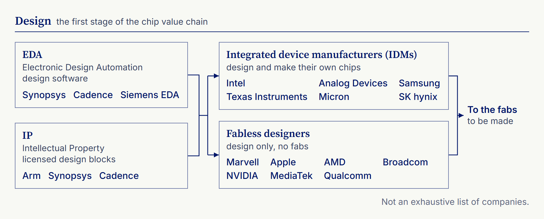
Making a chip takes a chain of companies, and design is the first link. The companies that design chips come in two kinds. An integrated device manufacturer (IDM), such as Intel, designs its chips and makes most of them in fabs of its own (since 2023 it has also had some parts of its processors made by TSMC).2.1 A fabless company, such as NVIDIA, only designs; its chips are made by a foundry, a company that manufactures chips to other companies’ designs.
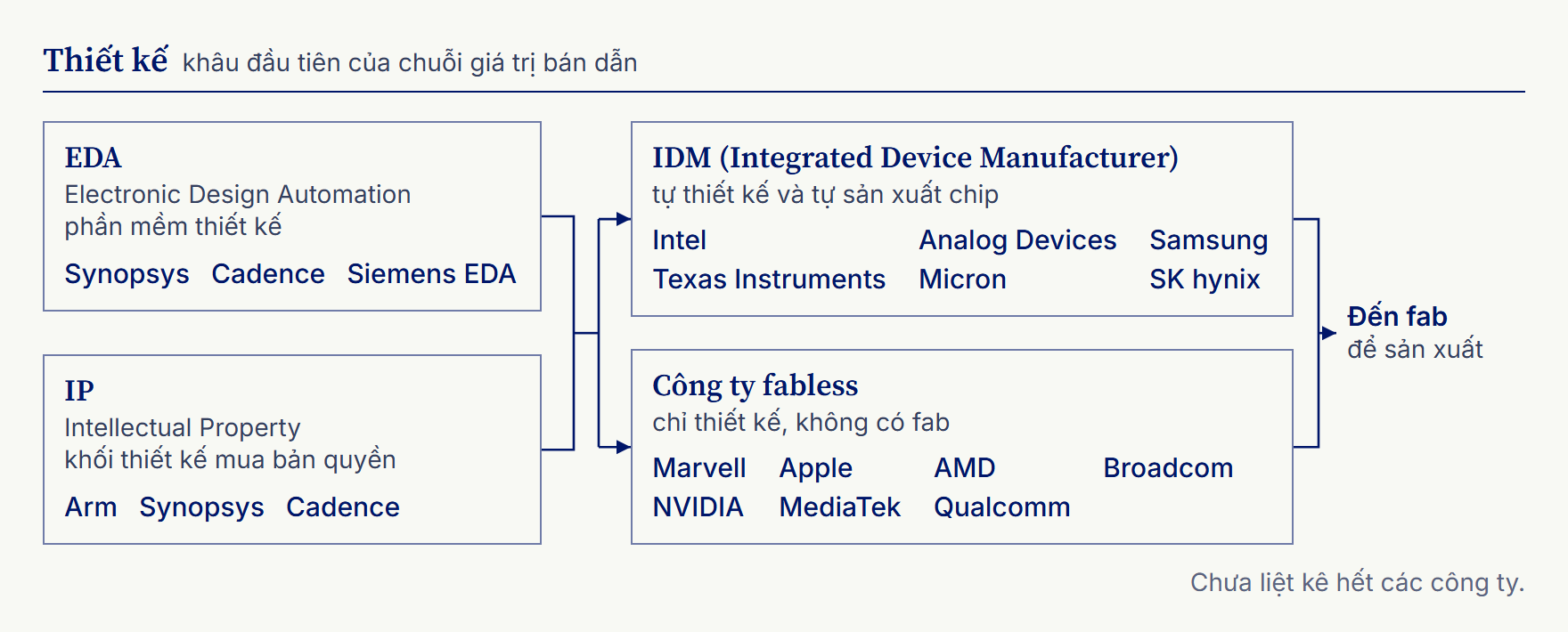
Làm ra một con chip cần cả một chuỗi công ty, và thiết kế là mắt xích đầu tiên. Các công ty thiết kế chip chia làm hai kiểu. Một IDM (integrated device manufacturer) như Intel vừa thiết kế chip vừa tự làm ra phần lớn số chip ấy trong nhà máy sản xuất chip (fab) của mình. Từ năm 2023, Intel cũng thuê TSMC làm một số phần trong bộ xử lý của hãng.2.1 Một công ty fabless như NVIDIA thì chỉ thiết kế, còn việc sản xuất giao cho một foundry, tức công ty chuyên sản xuất chip theo thiết kế của công ty khác.
Both kinds rely on suppliers that make no chips at all. Some sell electronic design automation (EDA) software, the programs in which a chip is drawn, simulated and checked; most of it, about nine tenths of the market in 2022, comes from three companies, Synopsys, Cadence Design Systems and Siemens EDA.2.2 Others license intellectual property (IP): finished pieces of design, such as a processor core, that a chip company pays to use instead of drawing them again. Arm, Synopsys and Cadence all sell IP.2.3
Cả hai kiểu đều dựa vào những nhà cung cấp không làm ra con chip nào. Một nhóm bán EDA (phần mềm thiết kế chip), tức những chương trình dùng để vẽ, mô phỏng và kiểm tra con chip. Khoảng chín phần mười thị trường này (năm 2022) thuộc về ba công ty Synopsys, Cadence Design Systems và Siemens EDA.2.2 Nhóm kia cấp phép IP (khối thiết kế mua bản quyền): những phần thiết kế làm sẵn, như một lõi xử lý, mà công ty chip trả tiền để dùng thay vì tự vẽ lại từ đầu. Arm, Synopsys và Cadence đều bán IP.2.3
A designer starts with EDA, IP and the PDK
Người thiết kế bắt đầu từ ba thứ: EDA, IP và PDK
A designer starts with three things that others have made. EDA software is the workbench: no chip of today could be designed without it, for reasons chapter 3 makes plain. IP spares a team from drawing again what others have already built and tested. The third, the foundry’s design kit, is the easiest to overlook.
Người thiết kế bắt đầu với ba thứ do người khác làm ra. Phần mềm EDA là bàn làm việc: không có nó thì không con chip nào ngày nay thiết kế nổi, vì những lý do chương 3 sẽ nói rõ. IP giúp một nhóm khỏi phải vẽ lại những gì người khác đã làm và thử nghiệm kỹ. Thứ ba là bộ tài liệu thiết kế của nhà máy, thứ dễ bị bỏ qua nhất.
A designer does not invent the transistor. The foundry that will make the chip has already worked out how each transistor, resistor and capacitor behaves in its own process, and it hands that knowledge over as a process design kit (PDK): models to simulate each device, templates to draw it, and the rules the drawing must obey.2.4 An analog or custom designer chooses the size of each transistor and how they connect; a digital designer works one level up, with ready-made cells built from those transistors (chapter 3). Chapter 5 shows a power chip built from a PDK’s devices in the first way.
Người thiết kế không tự nghĩ ra bóng bán dẫn (transistor). Chính foundry, nơi sẽ sản xuất con chip, đã tính sẵn xem từng transistor, điện trở, tụ điện hoạt động ra sao trên quy trình của mình. Họ trao lại những hiểu biết ấy dưới dạng một PDK (bộ tài liệu thiết kế của nhà máy): mô hình để mô phỏng từng linh kiện, bản vẽ mẫu để vẽ nó, và các quy tắc mà bản vẽ phải tuân theo.2.4 Người làm thiết kế tương tự (analog design) hay thiết kế riêng (custom) chọn kích thước cho từng transistor và nối chúng lại với nhau. Người làm thiết kế số (digital design) thì làm ở một tầng cao hơn, với những cell làm sẵn dựng từ các transistor ấy (chương 3). Chương 5 cho thấy một chip nguồn dựng lên từ chính các linh kiện trong PDK theo cách thứ nhất.
| Design software (EDA) | Licensed blocks (IP) | The foundry’s kit (PDK) | |
|---|---|---|---|
| Who supplies it | Software companies such as Synopsys, Cadence and Siemens EDA | IP companies such as Arm, Synopsys and Cadence | The foundry that will make the chip |
| What the designer gets | Programs to draw a circuit, simulate it, lay it out and check it | Tested blocks, such as a processor core or the circuit behind a USB port | The foundry’s devices: models to simulate them, templates to draw them, the rules a layout must obey |
| What is left to the designer | The design itself | The parts that make the chip different from others | For analog and custom blocks, the size of each transistor and how they connect; for digital blocks, which ready-made cells to use |
| Phần mềm thiết kế (EDA) | Khối thiết kế mua bản quyền (IP) | Bộ tài liệu thiết kế của nhà máy (PDK) | |
|---|---|---|---|
| Ai cung cấp | Các hãng phần mềm như Synopsys, Cadence, Siemens EDA | Các hãng IP như Arm, Synopsys, Cadence | Foundry sẽ sản xuất con chip |
| Người thiết kế nhận được gì | Chương trình để vẽ mạch, mô phỏng, làm layout và kiểm tra | Những khối đã được kiểm nghiệm, như một lõi xử lý hay mạch điều khiển cổng USB | Linh kiện của foundry: mô hình để mô phỏng, bản vẽ mẫu để vẽ, và các quy tắc mà layout phải tuân theo |
| Phần việc còn lại của người thiết kế | Chính bản thiết kế | Những phần làm nên nét riêng của con chip | Với khối analog và custom: kích thước từng transistor và cách nối chúng; với khối digital: dùng những cell làm sẵn nào |
Nine steps from a spec to a packaged chip
Chín bước biến yêu cầu kỹ thuật thành con chip đã đóng gói
With those in hand, a design goes through nine steps, drawn in plate 2.2 in a commonly used order.2.5
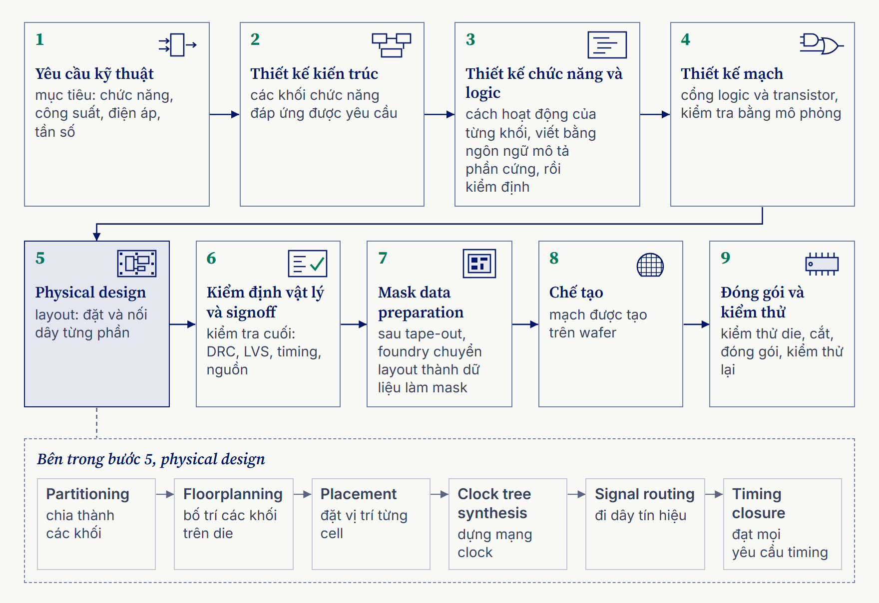
Khi đã có đủ những thứ ấy trong tay, người thiết kế đưa bản thiết kế đi qua chín bước; hình 2.2 vẽ chúng theo một thứ tự thường được dùng.2.5
It begins with the specification (step 1): what the product needs from the chip, written down as targets for its function, its power, its supply voltage and its operating frequency. Architecture (step 2) draws up the chip architecture, a plan that can meet those targets: which functional blocks the chip needs, each doing one job, and how they connect. Functional and logic design (step 3) sets out how each block behaves; for a digital block, that behaviour is written in a hardware language, the subject of chapter 3. Before a block goes further, its behaviour is checked against the specification, a stage called verification. The checking is done mostly by simulation, running the design through thousands to millions of test cases, and some of its properties are also proved mathematically. On a large chip this checking takes about as many engineers as the design itself (chapter 3).
Mọi thứ bắt đầu từ bước 1, yêu cầu kỹ thuật (specification): sản phẩm cần gì ở con chip, ghi thành các mục tiêu về chức năng, công suất, điện áp nguồn và tần số hoạt động. Bước 2, thiết kế kiến trúc, vạch ra kiến trúc chip, tức bản kế hoạch đáp ứng được các mục tiêu ấy: con chip cần những khối chức năng nào, mỗi khối đảm nhận một việc, và các khối nối với nhau ra sao. Bước 3, thiết kế chức năng và logic, xác định từng khối hoạt động thế nào; với khối digital, người ta viết cách hoạt động ấy bằng một ngôn ngữ mô tả phần cứng, chủ đề của chương 3. Trước khi đi tiếp, cách hoạt động của mỗi khối được đối chiếu với yêu cầu kỹ thuật, khâu gọi là kiểm định (verification). Việc kiểm tra chủ yếu dựa vào mô phỏng, cho thiết kế chạy qua hàng nghìn đến hàng triệu tình huống thử; một số tính chất của thiết kế còn được chứng minh bằng toán học. Trên một con chip lớn, khâu này cần số kỹ sư xấp xỉ số người thiết kế (chương 3).
Circuit design (step 4) turns each block into a circuit: a digital block’s code is mapped onto ready-made logic gates by logic synthesis (chapter 3), while analog and custom blocks are drawn transistor by transistor. Each is checked again by simulation: signals are fed to the circuit on a computer, and its outputs are compared with what it should do. After synthesis, a tool also confirms that the gates do exactly what the code did.
Thiết kế mạch (bước 4) biến mỗi khối thành một mạch điện. Với khối digital, code được chuyển thành các cổng logic làm sẵn bằng tổng hợp logic (synthesis), bước mà chương 3 sẽ nói kỹ; còn các khối analog và custom thì được vẽ tới từng transistor. Khối nào cũng lại được kiểm tra bằng mô phỏng: đưa tín hiệu vào mạch ngay trên máy tính và so đầu ra với những gì mạch phải làm. Sau bước synthesis, một công cụ còn xác nhận các cổng logic làm đúng hệt như code.
Physical design (step 5) is the layout, the exact drawing of every part, placed and wired. It has six steps of its own, in the plate’s dashed band. Partitioning splits the chip into regions, floorplanning arranges its large blocks on the die and plans the wiring that carries power to them, placement gives every cell (a small ready-made circuit, chapter 3) its spot, clock tree synthesis builds the network that carries the clock, signal routing draws the wires, and timing closure, which runs alongside the other steps, adjusts them until every signal arrives in time.2.6, 2.7
Physical design (bước 5) là layout, tức bản vẽ chính xác của từng bộ phận, đã đặt chỗ và nối dây xong. Riêng bước này đã gồm sáu bước nhỏ, nằm trong khung nét đứt của hình. Partitioning chia con chip thành từng vùng, floor planning sắp xếp các khối lớn trên die và vạch đường dây cấp nguồn cho chúng, placement đặt chỗ cho từng cell (một mạch nhỏ làm sẵn, xem chương 3). Tiếp đó, clock tree synthesis dựng mạng dẫn clock, và signal routing đi dây tín hiệu. Timing closure chạy song song với các bước kia, điều chỉnh chúng cho tới khi mọi tín hiệu đều đến kịp.2.6, 2.7
Physical verification and signoff (step 6) is the last round of checks before the design leaves. Physical verification asks whether the layout obeys the foundry’s design rules, such as the smallest widths and spacings its process can make, and whether it still matches the circuit. The signoff checks add timing and power: with the real wires now counted, every signal must still arrive on time, neither too late nor too early, even at the extremes of manufacturing variation, supply voltage and temperature, and the supply wiring must carry its current without too large a drop. When every check passes, the team signs the design off.2.5, 2.8
Bước 6, kiểm định vật lý (physical verification) và signoff, là vòng kiểm tra cuối cùng trước khi bản thiết kế rời đi. Physical verification soát xem layout có tuân theo các quy tắc thiết kế (design rule) của foundry không, và có còn khớp với mạch không. Design rule là những ràng buộc như độ rộng và khoảng cách nhỏ nhất mà quy trình của foundry làm được. Các bước kiểm tra signoff xét thêm timing và nguồn. Khi đã tính đủ dây nối thật, mọi tín hiệu vẫn phải đến đúng lúc, không muộn cũng không sớm, kể cả ở những tổ hợp cực đoan nhất của sai lệch sản xuất, điện áp nguồn và nhiệt độ. Mạng dây cấp nguồn cũng phải tải được dòng điện mà không sụt áp quá mức. Khi mọi bước đều đạt, nhóm thiết kế ký xác nhận (sign off) cho bản thiết kế.2.5, 2.8
When signoff is done, the finished layout leaves its designers’ hands as a file sent to the foundry, a hand-over called tape-out. Mask data preparation (step 7) is the foundry’s first job: it turns that layout into the data for the masks, the stencils that print each layer of the chip onto the wafer, adjusting the shapes so that they print as drawn.2.5, 2.9 The chip is then made. Fabrication (step 8) builds the circuits on wafers, and packaging and test (step 9) tests each die while it is still on the wafer, cuts the dies apart, seals the good ones in their packages, as chapter 1 described, and tests each packaged chip again.
Khi signoff xong, layout hoàn chỉnh rời tay người thiết kế dưới dạng một tệp gửi tới foundry; lần bàn giao ấy gọi là tape-out. Bước 7, mask data preparation (chuẩn bị dữ liệu mask), là việc đầu tiên của foundry: chuyển layout ấy thành dữ liệu để làm mask, những khuôn dùng để in từng lớp của con chip lên wafer. Các hình mẫu cũng được chỉnh lại để khi in ra, chúng đúng như bản vẽ.2.5, 2.9 Sau đó mới đến lượt làm ra con chip. Bước 8, chế tạo, dựng mạch trên wafer. Ở bước 9, đóng gói và kiểm thử, từng die được kiểm thử ngay khi còn trên wafer rồi mới cắt rời; die đạt thì được đóng gói như chương 1 đã kể, và mỗi con chip đóng gói xong lại qua một lần kiểm thử nữa.
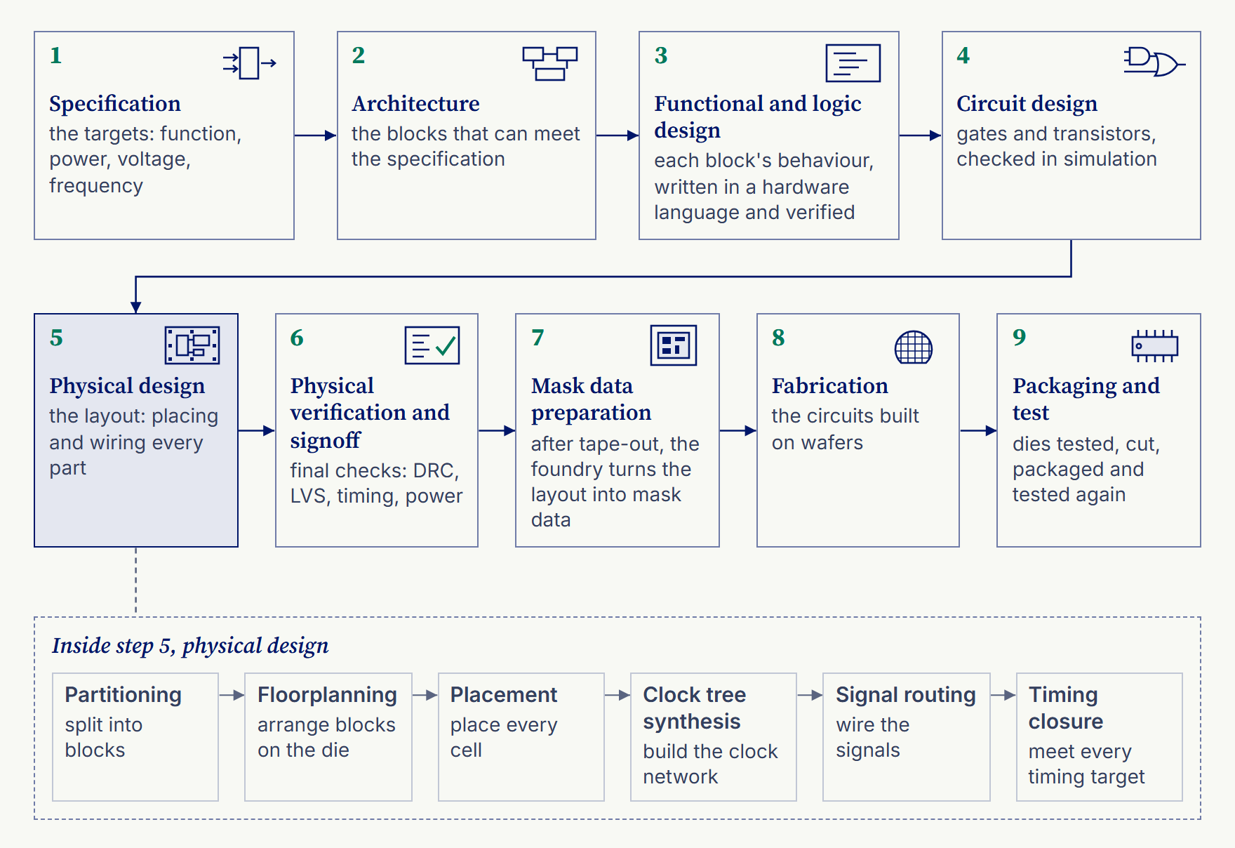
On the plate the arrows run one way. In practice, a check that fails sends the design back a step, sometimes several. Each case later in the book says where it stands on this map.
Trên hình, mũi tên chỉ đi một chiều. Trong thực tế, một lần kiểm tra không đạt sẽ đẩy bản thiết kế lùi lại một bước, có khi nhiều bước. Mỗi tình huống ở các chương sau đều chỉ ra mình đang đứng ở đâu trên sơ đồ này.
A NOR gate at school, a chip at work
Trên lớp là một cổng NOR, ở công ty là cả một con chip
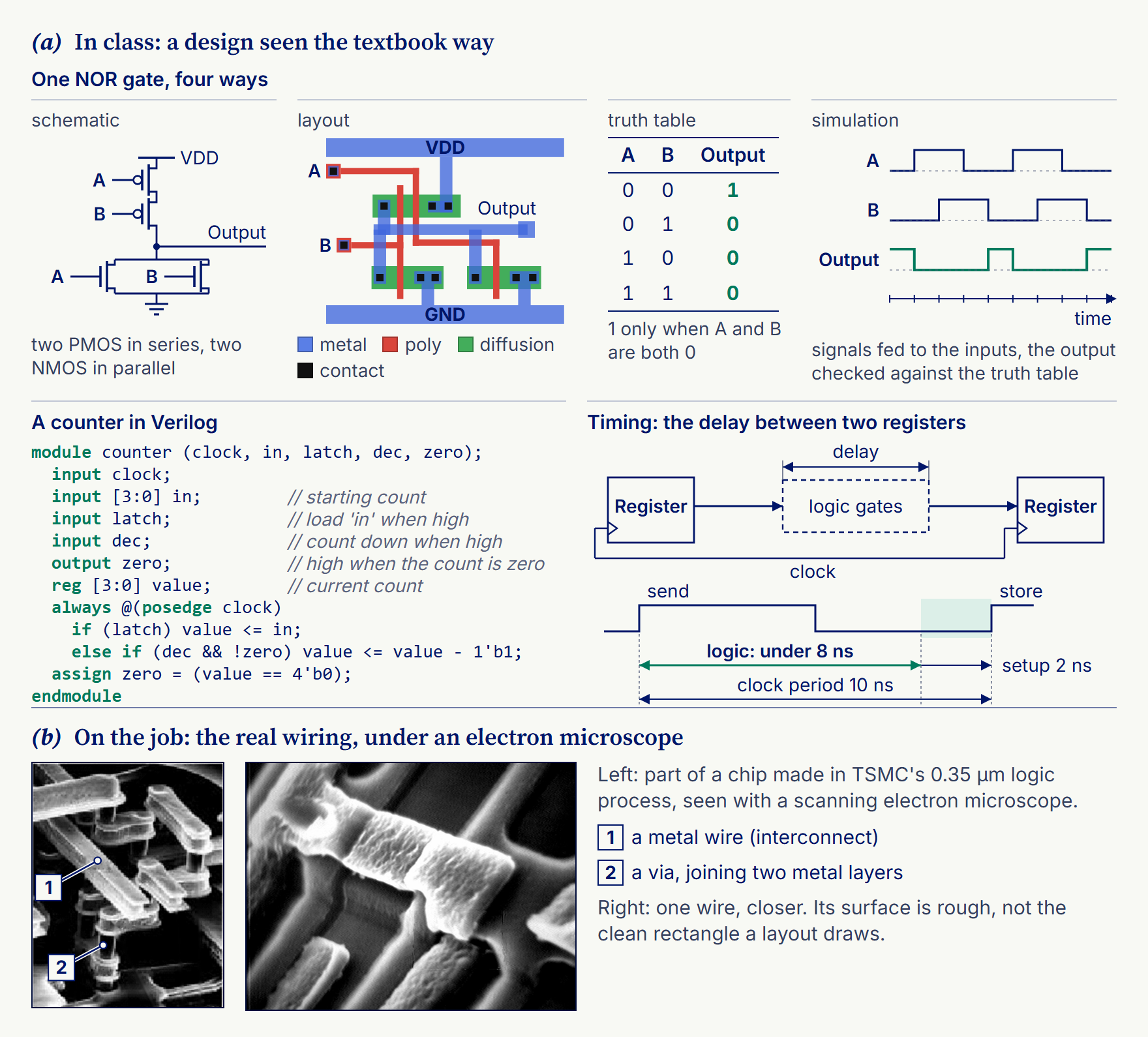
A flowchart is easy to learn and hard to picture. Plate 2.3 shows what the steps look like in class. Take one NOR gate, a logic gate whose output is 1 only when both inputs are 0. A course teaches it four ways: its schematic, two PMOS transistors in series and two NMOS in parallel; its layout, the shapes those transistors take when drawn; its truth table, the output for every pair of inputs; and a simulation that checks the output against the table.
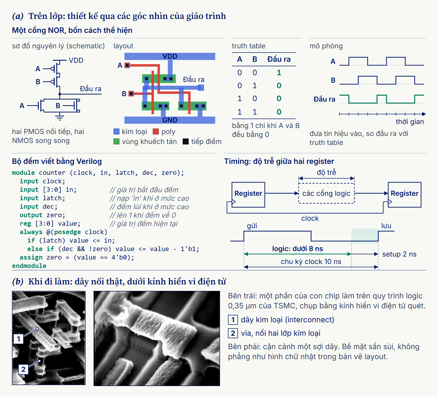
Sơ đồ quy trình thì dễ học nhưng khó hình dung. Hình 2.3 cho thấy trên lớp, các bước ấy trông ra sao. Lấy ví dụ một cổng NOR (NOR gate), cổng logic chỉ cho đầu ra bằng 1 khi cả hai đầu vào đều bằng 0. Môn học dạy cổng này theo bốn cách: sơ đồ nguyên lý (schematic), gồm hai transistor PMOS nối tiếp và hai NMOS song song; layout, tức hình dạng các transistor ấy khi vẽ ra; bảng chân lý (truth table), cho biết đầu ra ứng với từng cặp đầu vào; và mô phỏng để đối chiếu đầu ra với bảng.
The same plate shows a counter written in a hardware language, and the rule of timing every digital design lives by. A signal leaving one register must pass through the logic and reach the next register before the clock ticks again, with a little time to spare. With a clock period of 10 ns, and 2 ns that the next register needs to catch the signal (a round number for teaching; a modern register needs far less), the logic has less than 8 ns, because the signal also takes a moment to leave the first register, and the clock may reach the two registers at slightly different times. The rule has a second half: the signal must also not arrive so soon that it spoils what the next register is capturing.
Cũng trong hình là một bộ đếm (counter) viết bằng ngôn ngữ mô tả phần cứng, và quy tắc timing mà thiết kế digital nào cũng phải tuân theo. Tín hiệu rời một register phải đi qua phần logic và tới register kế tiếp trước khi clock gõ nhịp tiếp theo, còn dư một chút thời gian. Với chu kỳ clock 10 ns, trong đó register sau cần 2 ns để bắt được tín hiệu (một con số tròn để dạy học; register ngày nay cần ít hơn nhiều), phần logic chỉ còn chưa đầy 8 ns. Lý do là tín hiệu cũng mất một chút thời gian để rời register đầu, và clock có thể đến hai register vào những thời điểm hơi lệch nhau. Quy tắc này còn một nửa nữa: tín hiệu cũng không được tới quá sớm, làm hỏng dữ liệu mà register kế tiếp đang chốt.
At work the picture gets messier. A transistor as made is never exactly the transistor as drawn, and every wire slows a signal a little, so a design must allow for both if the chip is to work as intended once it is built. Under an electron microscope, a chip’s real wiring has rough surfaces and rounded corners (plate 2.3b), far from the perfect rectangles of a layout.
Ra đến thực tế, bức tranh lộn xộn hơn nhiều. Transistor làm ra không bao giờ giống hệt transistor trên bản vẽ, và mỗi đoạn dây lại làm tín hiệu chậm đi một chút. Thiết kế phải tính trước cả hai điều ấy thì con chip làm xong mới chạy đúng như dự định. Dưới kính hiển vi điện tử, dây nối thật trên chip có bề mặt sần sùi và góc bo tròn (hình 2.3b), khác xa những hình chữ nhật hoàn hảo trong layout.
School gives the clean views, and they are what make sense of the messy ones. An engineer who knows how a PMOS transistor works, and how it is drawn, can see why a real one behaves as it does.
Nhà trường cho ta những góc nhìn gọn gàng, và chính chúng giúp ta hiểu những gì ngổn ngang ngoài thực tế. Người kỹ sư đã biết một transistor PMOS hoạt động ra sao, vẽ ra trông thế nào, sẽ hiểu vì sao con transistor thật lại chạy như vậy.
Can one person design a whole chip?
Một người có thể thiết kế trọn một con chip không?
Can one person design a whole chip, from the specification to the file? It depends on the size of the chip. A small chip can be designed from start to finish by one person, as a student in a university lab often does (chapter 5). A chip of 200 billion transistors cannot. Its design is split among teams, and each team owns one part.
Một người có tự thiết kế trọn một con chip, từ yêu cầu kỹ thuật đến tệp thiết kế, được không? Còn tùy con chip lớn đến đâu. Một con chip nhỏ thì một người có thể thiết kế từ đầu đến cuối, như sinh viên trong phòng thí nghiệm đại học vẫn thường làm (chương 5). Con chip 200 tỷ transistor thì không. Việc thiết kế phải chia cho nhiều nhóm, mỗi nhóm phụ trách một phần.
That is where school and work part ways. At university a student does every step of the design, on small circuits. At a company an engineer may do one step, and do it for years. Each step can be a job of its own:
Đó cũng là chỗ nhà trường và công việc rẽ sang hai ngả. Ở đại học, sinh viên tự làm mọi bước thiết kế trên những mạch nhỏ. Ở công ty, một kỹ sư có thể chỉ làm một bước, và làm nó nhiều năm liền. Mỗi bước đều có thể thành một nghề riêng:
- Drawing circuits: the circuit design of step 4
- Drawing the layout, inside step 5
- Verification: checking, mostly by simulation, that a design does what its specification says
- Synthesis: turning a block’s code into logic gates (chapter 3)
- Lab work: measuring finished chips, opening them up and photographing them to find a defect
- Vẽ mạch: phần thiết kế mạch ở bước 4
- Vẽ layout, bên trong bước 5
- Verification: kiểm tra, chủ yếu bằng mô phỏng, xem thiết kế có làm đúng như yêu cầu kỹ thuật không
- Synthesis: chuyển code của một khối thành cổng logic (chương 3)
- Làm trong phòng thí nghiệm: đo những con chip đã làm xong, mở chúng ra, chụp ảnh để tìm chỗ hỏng
None of these is a lesser job, and none is a dead end. They all rest on the same fundamentals, and the fundamentals are what let an engineer move on: someone who starts in the lab may, after many years and with enough persistence, go on to design a chip’s architecture, step 2. So the years at university are best spent on as broad a base as possible; the narrow part comes with the job.
Không việc nào trong số đó kém giá trị hơn, và cũng không việc nào là ngõ cụt. Tất cả đều dựa trên cùng một nền tảng, và chính nền tảng ấy cho phép người kỹ sư đi tiếp. Người bắt đầu trong phòng thí nghiệm, sau nhiều năm và nếu đủ bền bỉ, có thể chuyển sang thiết kế kiến trúc chip, tức bước 2. Vì thế, những năm đại học đáng dành để xây nền tảng càng rộng càng tốt; phần chuyên sâu sẽ đến cùng công việc.
The next chapter follows steps 3 to 6 through a digital chip of billions of transistors, up to the hand-over at tape-out; chapters 4 and 5 take the same flow into analog design.
Chương sau theo chân các bước 3 đến 6 trên một con chip digital có hàng tỷ transistor, cho tới lần bàn giao ở tape-out; chương 4 và 5 đưa chính quy trình ấy sang thiết kế analog.