Chapter 4 of 10Chương 4/10 11 min11 phút
Powering an AI processorCấp nguồn cho bộ xử lý AI
A processor does its work with billions of transistors, and every one of them needs power at the right voltage, the moment it asks for it. Getting that power there is a design problem of its own. This chapter and the next follow how one university lab, the iPower3Es lab at UC San Diego, designs a power chip for an AI processor, worked here against an illustrative specification rather than a real product’s.4.1 This chapter covers the first two steps of the design flow in chapter 2, the specification and the architecture; chapter 5 follows the steps after them, down to transistors, a layout and a test board.
Một bộ xử lý làm việc bằng hàng tỷ bóng bán dẫn (transistor), và transistor nào cũng cần được cấp điện đúng mức điện áp, đúng lúc nó cần. Đưa được nguồn điện ấy tới nơi là cả một bài toán thiết kế riêng. Chương này và chương sau dõi theo cách một phòng thí nghiệm đại học, iPower3Es lab ở UC San Diego, thiết kế chip nguồn cho bộ xử lý AI. Ở đây, con chip được thiết kế theo một bản yêu cầu kỹ thuật (specification) minh họa, chứ không phải theo thông số của một sản phẩm có thật.4.1 Chương này đi qua hai bước đầu của quy trình thiết kế (design flow) ở chương 2, là yêu cầu kỹ thuật và kiến trúc; chương 5 đi tiếp các bước sau đó, xuống tới từng transistor, bản layout và bo mạch thử.
In this chapter
Trong chương này
- What a power-management chip does, and why every board carries several
- Why an AI processor needs its power chips right beside it
- What a worked specification for one supply rail asks for
- How three candidate circuits were screened
- Why a three-level converter needs less inductance for the same ripple
- Chip quản lý năng lượng làm gì, và vì sao bo mạch nào cũng mang vài con
- Vì sao bộ xử lý AI cần chip nguồn đặt ngay sát bên
- Bản yêu cầu kỹ thuật minh họa cho một đường cấp nguồn đòi hỏi những gì
- Ba cấu trúc mạch được sàng lọc ra sao
- Vì sao bộ chuyển đổi ba mức cần độ tự cảm nhỏ hơn cho cùng một độ gợn
Every chip needs power
Con chip nào cũng cần được cấp nguồn
A power-management integrated circuit (PMIC) turns whatever supply a device has, a battery or the output of a bigger power unit, into the exact voltages its other chips need, and holds each one steady. Parts that need different voltages get separate supply lines, each a power rail fed by a voltage regulator: a circuit that keeps its output at a set voltage however the input and the load change, as long as they stay within the range it is built for.
Chip quản lý năng lượng (PMIC) biến nguồn điện sẵn có của thiết bị, là viên pin hay đầu ra của một bộ nguồn lớn hơn, thành đúng những mức điện áp mà các con chip khác cần, rồi giữ cho từng mức ổn định. Những bộ phận cần điện áp khác nhau thì có đường nguồn riêng, mỗi đường là một đường cấp nguồn (power rail) do một bộ ổn áp (voltage regulator) cấp điện. Bộ ổn áp là mạch giữ điện áp ra ở một giá trị đặt trước dù điện áp vào hay tải thay đổi, miễn là các thay đổi ấy vẫn nằm trong phạm vi thiết kế của nó.
So power chips sit on every board, from a phone to an accelerator card in a data center. On the iPhone Air’s logic board, four of them are easy to pick out.4.2 On the board of an NVIDIA H100, a GPU built for data centers, rows of voltage regulators surround the GPU package on all four sides.
Bởi vậy bo mạch nào cũng có chip nguồn, từ chiếc điện thoại đến card accelerator trong data center. Trên bo mạch logic của iPhone Air, có thể chỉ ra ngay bốn con chip nguồn.4.2 Trên bo mạch của NVIDIA H100, một GPU làm riêng cho data center, các hàng bộ ổn áp vây quanh package (phần đóng gói của chip) của GPU ở cả bốn phía.
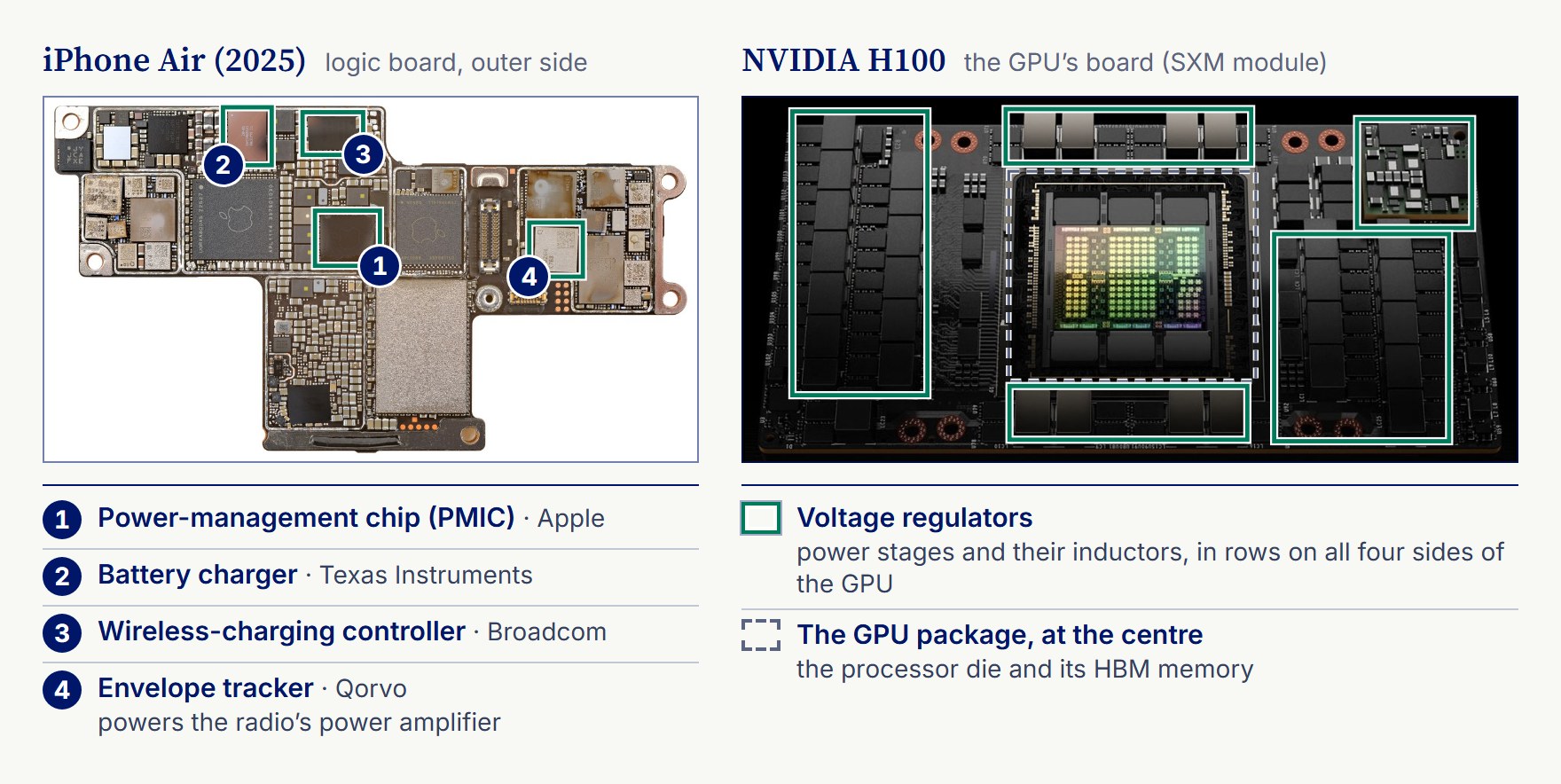
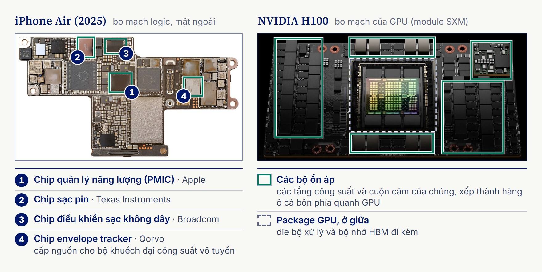
Power chips are an old technology. One of the first integrated voltage regulators, Fairchild Semiconductor’s μA723, came out in 1967. The first chip made to control a switching regulator, Silicon General’s SG1524, followed in 1976.4.3, 4.4 For decades a power chip was a part of its own, a regulator or a battery charger in its own package, bought off the shelf and soldered onto the board beside whatever it fed. What has changed is what it feeds.
Chip nguồn là một công nghệ lâu đời. Một trong những bộ ổn áp tích hợp đầu tiên, μA723 của Fairchild Semiconductor, ra đời năm 1967. Con chip đầu tiên dùng để điều khiển bộ ổn áp xung (switching regulator), SG1524 của Silicon General, có mặt năm 1976.4.3, 4.4 Suốt mấy chục năm, chip nguồn là một linh kiện đứng riêng: một bộ ổn áp hay một chip sạc pin trong package của riêng nó, mua sẵn về rồi hàn lên bo mạch, cạnh bộ phận mà nó cấp điện. Nhưng thứ mà nó cấp điện thì đã khác xưa.
Why the power chip moved next to the processor
Vì sao chip nguồn phải dời đến sát bộ xử lý
Today an AI processor draws so much current, at so low a voltage, that the path from its regulator has to be as short as possible. Early PC processors ran from one standard supply (5 V for the 486 and the first Pentium, 3.3 V for the later Pentiums), and an off-the-shelf regulator chip could provide it: the computer maker simply bought the chip and put it on the board.4.5, 4.6 Core voltages have since fallen to around 1 V and below, and one processor now needs many supplies at once. A server processor needs dozens of separate power rails, each at its own voltage.4.7 By 2024 a data-center AI GPU drew around 1,000 W: NVIDIA’s B200, for one, is configurable up to 1 kW per GPU.4.8 And the number is still climbing: at ISSCC 2025, the main conference for chip circuits, Intel looked ahead to packages delivering 1 to 2 kW and more.4.9
Bộ xử lý AI ngày nay kéo dòng điện rất lớn ở điện áp rất thấp, nên đường dẫn điện từ bộ ổn áp tới nó phải càng ngắn càng tốt. Bộ xử lý của máy tính cá nhân đời đầu chỉ chạy bằng một mức nguồn chuẩn (5 V với dòng 486 và chiếc Pentium đầu tiên, 3,3 V với các đời Pentium sau đó), và một con chip ổn áp bán sẵn là đáp ứng được. Hãng làm máy tính chỉ việc mua chip về, gắn lên bo mạch.4.5, 4.6 Từ đó đến nay, điện áp lõi đã xuống quanh 1 V và thấp hơn nữa, còn mỗi bộ xử lý nay cần nhiều mức nguồn cùng lúc. Một bộ xử lý máy chủ cần tới hàng chục đường nguồn riêng, mỗi đường một mức điện áp.4.7 Tới năm 2024, một GPU AI trong data center đã tiêu thụ khoảng 1.000 W: B200 của NVIDIA, chẳng hạn, có thể cấu hình tới 1 kW cho mỗi GPU.4.8 Và con số ấy vẫn đang tăng: tại ISSCC 2025, hội nghị hàng đầu về vi mạch, Intel đã tính tới những package cấp được từ 1 đến 2 kW, thậm chí hơn nữa.4.9
Low voltage and high power make a hard mix. Power is voltage times current, so a kilowatt delivered at around 1 V means a current approaching a thousand amperes.4.10 Every piece of copper between the regulator and the processor has a little resistance and a little inductance. At that current even a tiny resistance wastes power as heat. And when the processor’s demand jumps, the path’s inductance holds back the extra current for a moment, so the voltage dips until the regulator catches up. The shorter the path, the smaller both are.
Điện áp thấp mà công suất lại lớn: đó là một bài toán khó. Công suất bằng điện áp nhân với dòng điện, nên muốn cấp một kilowatt ở khoảng 1 V thì dòng điện phải lên tới gần một nghìn ampe.4.10 Mọi đoạn đồng nằm giữa bộ ổn áp và bộ xử lý đều có một chút điện trở và một chút độ tự cảm. Với dòng điện lớn như thế, chỉ một điện trở rất nhỏ cũng đủ biến công suất thành nhiệt. Còn khi bộ xử lý đột ngột đòi thêm dòng, độ tự cảm của đường dẫn kìm dòng điện lại trong chốc lát, nên điện áp tụt xuống cho tới khi bộ ổn áp kịp đáp ứng. Đường đi càng ngắn thì cả hai càng nhỏ.
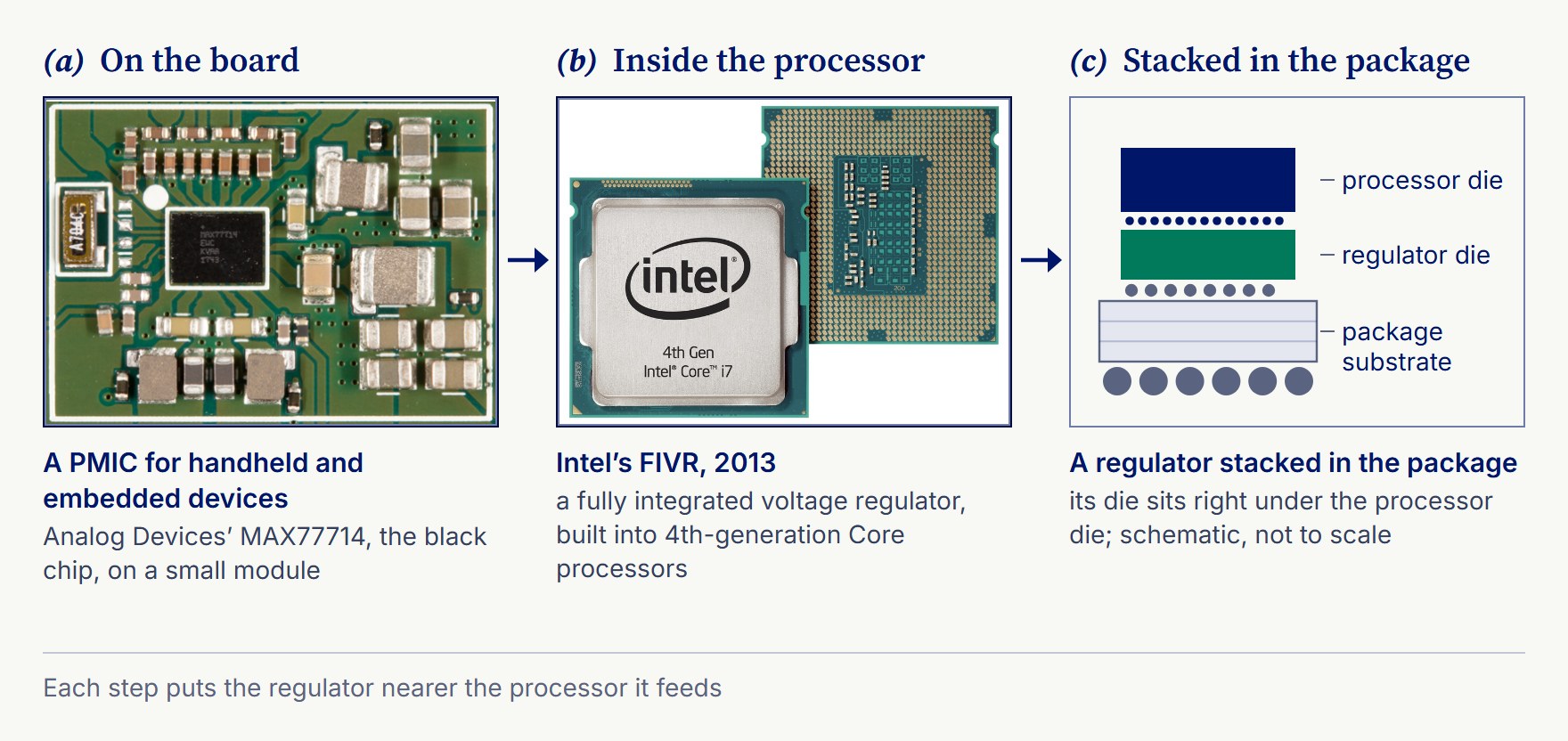
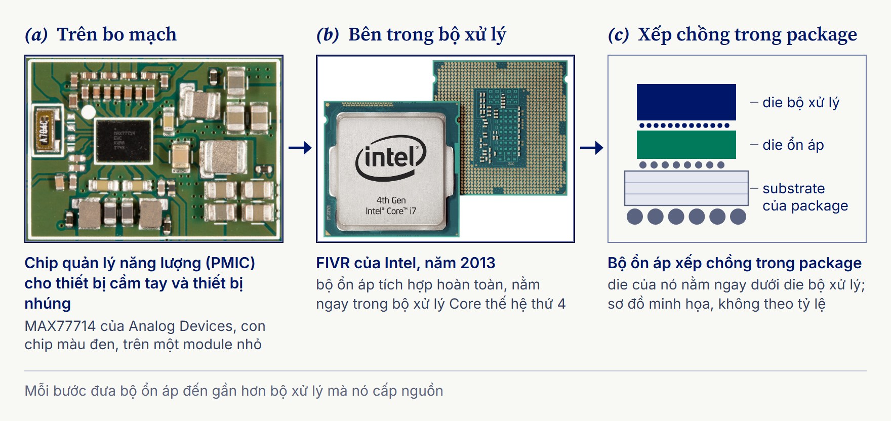
So the regulator has moved closer in steps, as the plate below shows. First it sat on the board, as a PMIC beside the processor, like the one made for handheld and embedded devices in part (a).4.11 Then most of it moved inside the processor itself: Intel built a fully integrated voltage regulator (FIVR) into its 4th-generation Core processors in 2013, with its switches on the processor’s silicon and its inductors in the package.4.12 The latest step puts the regulator in the processor’s own package. A multi-chip package holds two or more dies, the bare pieces of silicon, side by side or stacked, so a processor and its regulator can share one package; that is one of the jobs of advanced packaging.
Thế nên bộ ổn áp đã tiến lại gần qua từng bước, như hình dưới đây cho thấy. Đầu tiên nó nằm trên bo mạch, là một PMIC đặt cạnh bộ xử lý, như con chip dành cho thiết bị cầm tay và thiết bị nhúng ở phần (a).4.11 Sau đó phần lớn bộ ổn áp vào hẳn bên trong bộ xử lý: Intel tích hợp FIVR (fully integrated voltage regulator), một bộ ổn áp nằm ngay trong chip, vào dòng bộ xử lý Core thế hệ thứ 4 năm 2013; các khóa của nó nằm ngay trên phần silicon của bộ xử lý, còn cuộn cảm nằm trong package.4.12 Bước mới nhất đưa bộ ổn áp vào ngay trong package của bộ xử lý. Một multi-chip package chứa từ hai die trở lên, tức những mẩu silicon trần, đặt cạnh nhau hoặc xếp chồng, nhờ vậy bộ xử lý và bộ ổn áp của nó có thể nằm chung một package; đó là một trong những việc của đóng gói tiên tiến (advanced packaging).
That move has changed the power-chip designer’s job. For a processor like this, power delivery can no longer be left to the end, as parts to be bought and added on once the processor is done. Power-chip designers now join the architecture work for the whole system, alongside the processor’s designers, so that the finished product computes fast and uses its energy well. An old field has found new work: a power die packaged right beside a high-performance computing (HPC) die is still a young area of research.
Bước chuyển ấy cũng làm thay đổi công việc của người thiết kế chip nguồn. Với một bộ xử lý như thế, việc cấp nguồn không còn là thứ để đến cuối mới lo, như những linh kiện mua về rồi gắn thêm khi bộ xử lý đã xong. Người thiết kế PMIC nay tham gia ngay từ khâu thiết kế kiến trúc của cả hệ thống, cùng với những người thiết kế bộ xử lý, để sản phẩm cuối cùng vừa tính toán nhanh vừa dùng năng lượng hiệu quả. Một lĩnh vực lâu đời nhờ vậy lại có thêm đất dụng võ: đặt die nguồn ngay cạnh die tính toán hiệu năng cao (HPC) vẫn là một hướng nghiên cứu còn non trẻ.
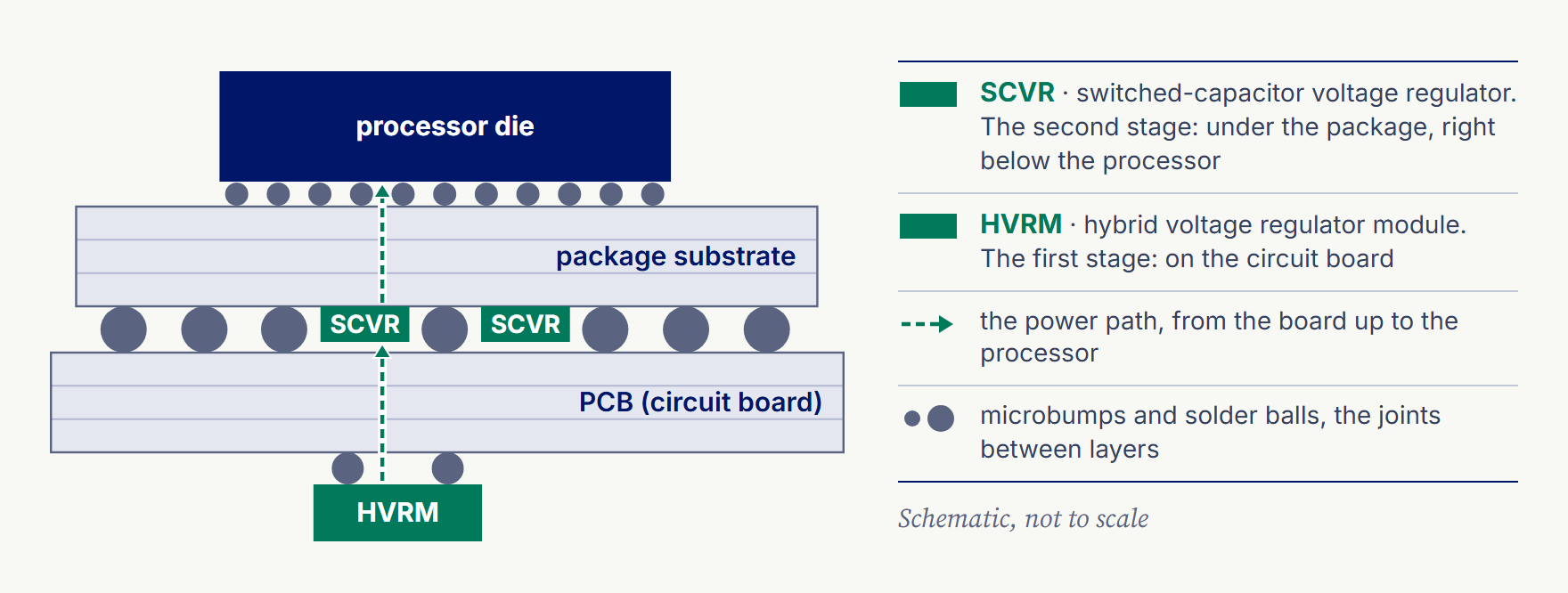
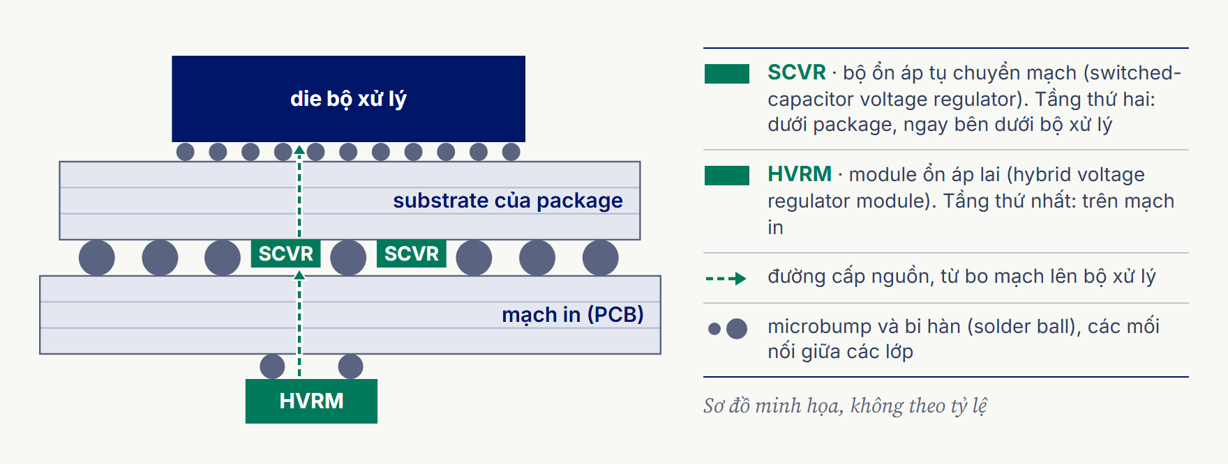
With currents this large, one way to bring power to the processor is in two stages. The lab behind this case built and measured such a design, published at ISSCC 2023. Its first stage, a hybrid voltage regulator module (HVRM) on the circuit board, turns a 12 to 20 V supply into about 4 V. Its last stage, a set of switched-capacitor voltage regulators (SCVR) mounted under the package right below the processor die, divides that by four, to about 1 V.4.13
Với dòng điện lớn như vậy, một cách để đưa điện tới bộ xử lý là chia làm hai tầng. Chính phòng thí nghiệm đứng sau tình huống này đã làm ra và đo đạc một thiết kế như vậy, công bố tại ISSCC 2023. Tầng thứ nhất là một HVRM (hybrid voltage regulator module), module ổn áp lai, đặt trên mạch in; nó hạ nguồn 12 đến 20 V xuống khoảng 4 V. Tầng cuối là các SCVR (switched-capacitor voltage regulator), bộ ổn áp tụ chuyển mạch, gắn ở mặt dưới package, ngay bên dưới die bộ xử lý. Chúng chia tiếp điện áp ấy cho bốn, xuống khoảng 1 V.4.13
Writing a specification for one power rail
Lập yêu cầu kỹ thuật cho một đường cấp nguồn
This case writes its specification for one rail only, an illustrative 10 W rail; the processor as a whole draws about 1 kW across many. Suppose a regulator sitting beside an AI processor must do the last stage’s job, turning 3 to 5 V into 0.8 to 1 V at 10 W; the table sets out the whole target.
Tình huống này chỉ lập yêu cầu kỹ thuật cho một đường nguồn, một đường 10 W để minh họa, trong khi cả bộ xử lý tiêu thụ khoảng 1 kW, chia trên nhiều đường nguồn. Giả sử một bộ ổn áp đặt cạnh bộ xử lý AI phải làm việc của tầng cuối, hạ 3 đến 5 V xuống 0,8 đến 1 V ở công suất 10 W; bảng dưới đây ghi đầy đủ các mục tiêu.
| The worked specification | Target |
|---|---|
| Input voltage | 3 to 5 V |
| Output voltage | 0.8 to 1 V |
| Power delivered | 10 W |
| Efficiency | above 95% |
| Area | 10 mm² |
| Thickness | 1 mm |
| Voltage droop, the dip when the load jumps | under 20 mV when the current jumps by 5 A in 20 ns |
| Package | a BGA or QFN package, or a place inside an advanced package whose dies are linked by silicon bridges, such as Intel’s EMIB |
| Manufacturing process | still to be chosen, for example TSMC at 22, 65 or 180 nm |
| Bản yêu cầu kỹ thuật minh họa | Mục tiêu |
|---|---|
| Điện áp vào | 3 đến 5 V |
| Điện áp ra | 0,8 đến 1 V |
| Công suất cấp cho tải | 10 W |
| Hiệu suất | trên 95% |
| Diện tích | 10 mm² |
| Độ dày | 1 mm |
| Sụt áp khi tải tăng đột ngột | dưới 20 mV khi dòng điện tăng thêm 5 A trong 20 ns |
| Kiểu đóng gói | package BGA hoặc QFN, hoặc một chỗ trong package tiên tiến có các die nối với nhau bằng cầu nối silicon, như EMIB của Intel |
| Quy trình sản xuất | chưa chốt, chẳng hạn TSMC ở 22, 65 hoặc 180 nm |
Two lines carry most of the difficulty. Efficiency, the share of the input power that reaches the load, must stay above 95%, an ambitious target: while 10 W reaches the load, only about half a watt may turn into heat, in a part about 3 mm on a side. And when the processor suddenly draws 5 A more, the output may dip by less than 20 mV, under 2% of a 1 V output. A specification like this is the first step of the design flow: it fixes what the chip must achieve before anyone decides how.
Hai dòng trong bảng gánh phần lớn cái khó. Hiệu suất, tức phần công suất đầu vào đến được tải, phải trên 95%, một mục tiêu đầy tham vọng: khi 10 W đến được tải, chỉ khoảng nửa watt được phép biến thành nhiệt, trên một linh kiện mỗi cạnh chừng 3 mm. Còn khi bộ xử lý bất ngờ kéo thêm 5 A, điện áp ra chỉ được tụt chưa tới 20 mV, chưa đến 2% của mức 1 V. Một bản yêu cầu như thế là bước đầu tiên trong quy trình thiết kế: nó chốt con chip phải đạt được những gì, trước khi bàn đến chuyện làm cách nào.
Choosing among three candidate circuits
Chọn một trong ba cấu trúc mạch
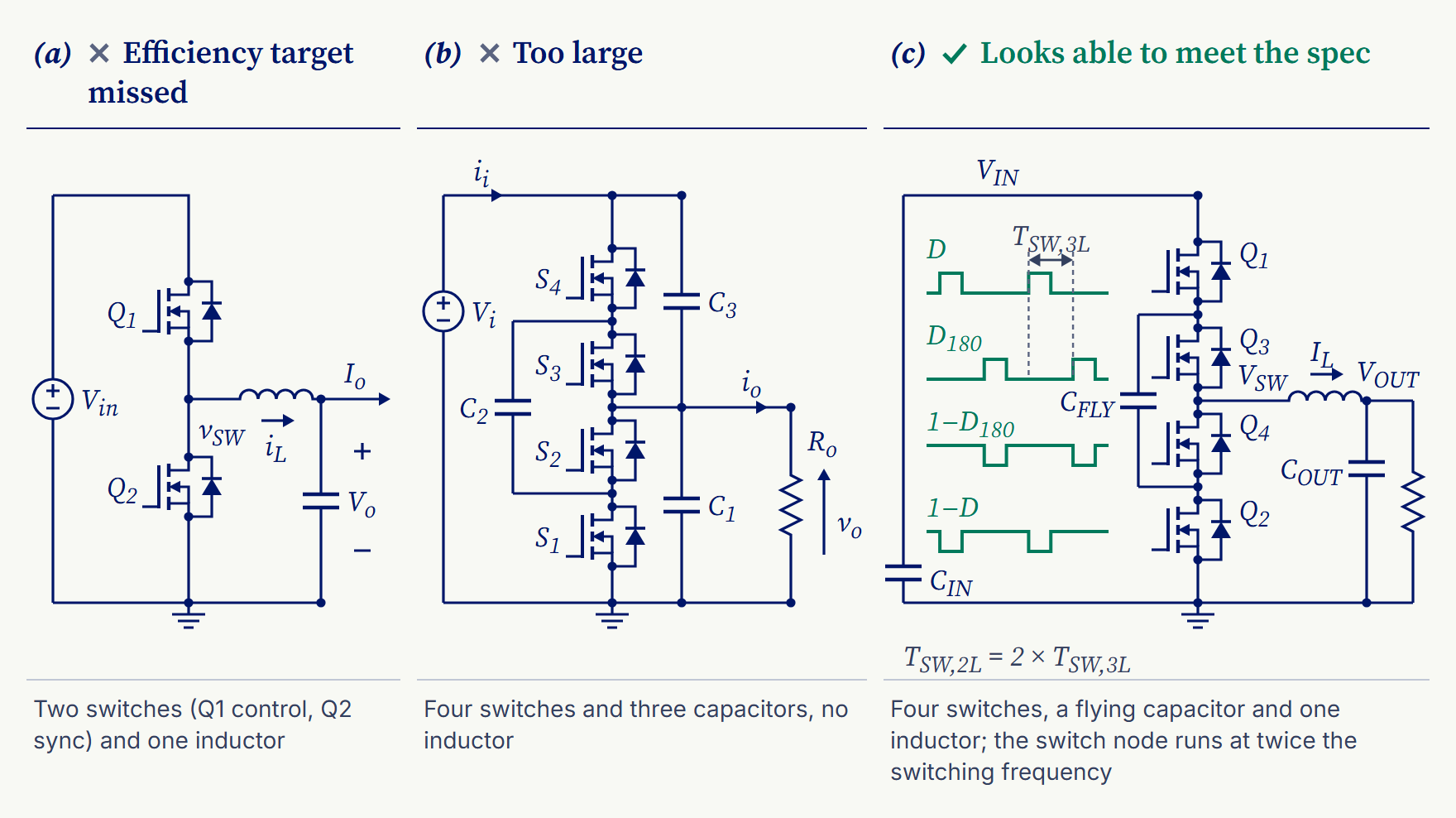
The second step, the architecture, decides which circuit can meet that target, and here power-chip design borrows from power electronics, the branch of electronics that converts power with switches. The designer picks a topology, the way the switches, capacitors and inductors are connected; counts how many of each it needs; and estimates whether it can reach the efficiency asked for, in the area allowed, on the chosen process. Many topologies are tried before one looks promising. This case screened three.
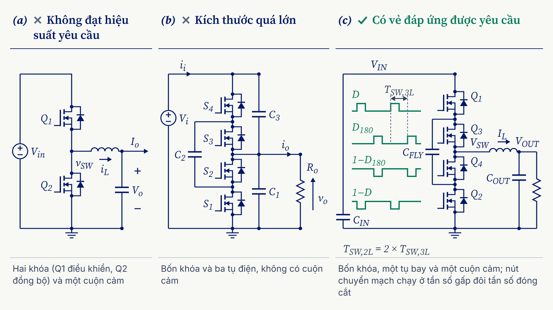
Bước thứ hai, thiết kế kiến trúc, quyết định mạch nào có thể đạt mục tiêu ấy, và ở bước này, thiết kế chip nguồn mượn nhiều kiến thức của điện tử công suất, ngành điện tử chuyên biến đổi điện năng bằng các khóa đóng cắt. Người thiết kế chọn một cấu trúc mạch (topology), tức cách nối các khóa, tụ điện và cuộn cảm với nhau; đếm xem mỗi loại linh kiện cần bao nhiêu; rồi ước lượng xem mạch có đạt hiệu suất yêu cầu, trong diện tích cho phép, trên quy trình sản xuất đã chọn hay không. Phải thử rất nhiều cấu trúc mạch mới thấy một cấu trúc có triển vọng. Trong tình huống này, ba mạch được đem ra sàng lọc.
The first is the buck converter, the standard circuit for lowering a DC voltage.4.14 Two transistor switches connect one point of the circuit, the switch node, to the input and then to ground in turn, at a switching frequency usually held fixed: a million times a second or more in a small converter like this one.4.15 An inductor and a capacitor smooth the chopped voltage into a steady output. The fraction of each period during which the upper switch is on, the duty cycle D, sets the output: ideally, Vout = D × Vin.
Mạch thứ nhất là bộ chuyển đổi buck (buck converter), mạch tiêu chuẩn để hạ một điện áp một chiều.4.14 Hai khóa transistor lần lượt nối một điểm trong mạch, gọi là nút chuyển mạch (switch node), với đầu vào rồi với đất, ở một tần số đóng cắt thường được giữ cố định: từ một triệu lần mỗi giây trở lên với một bộ chuyển đổi nhỏ như thế này.4.15 Cuộn cảm và tụ điện làm phẳng điện áp bị “băm” ấy thành một điện áp ra ổn định. Phần thời gian khóa phía trên dẫn trong mỗi chu kỳ, gọi là hệ số lấp đầy (duty cycle) D, quyết định điện áp ra: trong trường hợp lý tưởng, Vout = D × Vin.
The second, a switched-capacitor converter, has no inductor at all. Its switches charge capacitors and then reconnect them in a new arrangement, which divides the voltage by a fixed ratio, such as 2:1.
Mạch thứ hai, bộ chuyển đổi tụ chuyển mạch (switched-capacitor converter), hoàn toàn không có cuộn cảm. Các khóa nạp điện cho tụ rồi đấu các tụ lại theo một cách khác, nhờ đó điện áp được chia theo một tỷ lệ cố định, chẳng hạn 2:1.
The third, a three-level buck converter, is a buck with four switches instead of two and a flying capacitor between them: a capacitor whose two ends both move with the switches, held at half the input voltage by a control loop of its own. At duty cycles below one half, as throughout this specification, the switches take turns so that the switch node steps only between 0 and half the input, twice in every switching period.
Mạch thứ ba, bộ chuyển đổi buck ba mức (three-level buck converter), là một bộ buck dùng bốn khóa thay vì hai, với một tụ bay (flying capacitor) nằm giữa. Đó là tụ điện có cả hai đầu cùng thay đổi điện thế theo các khóa, được một vòng điều khiển riêng giữ ở một nửa điện áp vào. Với duty cycle nhỏ hơn một nửa, điều luôn đúng trong bản yêu cầu này, các khóa thay phiên nhau để nút chuyển mạch chỉ nhảy giữa 0 và một nửa điện áp vào, hai lần trong mỗi chu kỳ đóng cắt.
The screening came out like this: the buck missed the efficiency target, the switched-capacitor converter came out too large, and the three-level buck looked able to meet the specification. These are the case’s own results; no figures for the losses or the areas behind them have been published.
Kết quả sàng lọc như sau: bộ buck không đạt hiệu suất yêu cầu, bộ chuyển đổi tụ chuyển mạch có kích thước quá lớn, còn bộ buck ba mức có vẻ đáp ứng được yêu cầu kỹ thuật. Đây là kết quả riêng của tình huống này; các con số về tổn hao hay diện tích làm cơ sở cho những kết luận ấy chưa được công bố.
The physics behind the verdicts is standard. In the plain buck each switch blocks the whole input and switches it on every cycle, which costs energy each time. In the three-level buck each switch blocks only half the input, the switch node swings half as far, and the inductor sees twice the frequency.4.16
Còn lý do vật lý thì quen thuộc. Ở bộ buck thường, mỗi khóa phải chịu toàn bộ điện áp vào và đóng cắt nó ở mọi chu kỳ, lần nào cũng hao năng lượng. Ở bộ buck ba mức thì mỗi khóa chỉ chịu một nửa điện áp vào, nút chuyển mạch chỉ nhảy nửa quãng, còn cuộn cảm chịu tần số gấp đôi tần số đóng cắt.4.16
A switched-capacitor converter divides by a fixed ratio and is efficient only close to it. This specification’s 3 to 5 V input and 0.8 to 1 V output need ratios from 3 to more than 6, so one converter would need several ratios, and the extra switches and capacitors that go with them. In the lab’s published two-stage design the board stage hands the switched-capacitor stage 3.2 to 4.2 V, which it divides at one fixed ratio, 4:1. That board stage is itself a three-level buck.4.13
Bộ chuyển đổi tụ chuyển mạch chia điện áp theo một tỷ lệ cố định, và chỉ đạt hiệu suất cao khi chạy gần đúng tỷ lệ ấy. Với điện áp vào 3 đến 5 V và điện áp ra 0,8 đến 1 V, bản yêu cầu này đòi tỷ lệ từ 3 đến hơn 6, nên chỉ một bộ chuyển đổi thì phải có nhiều tỷ lệ, kéo theo thêm khóa và tụ điện. Trong thiết kế hai tầng mà phòng thí nghiệm đã công bố, tầng trên bo mạch đưa cho tầng tụ chuyển mạch điện áp 3,2 đến 4,2 V, và tầng này chỉ chia theo một tỷ lệ cố định, 4:1. Bản thân tầng trên bo mạch ấy là một bộ buck ba mức.4.13
What a three-level buck gains
Bộ buck ba mức có lợi thế gì so với bộ buck hai mức
What the three-level buck gains shows up in the inductor. In an ordinary buck, while the upper switch is on, the inductor has the whole input minus the output across it, and its current ramps up; while the lower switch is on, the current ramps back down. That up-and-down swing is the ripple the output capacitor has to absorb. In the three-level buck the switch node climbs only to half the input, so for the same on-time the inductor sees half the input minus the output, a much smaller voltage. Its current ramps more gently, and the ripple shrinks.
Cái lợi của bộ buck ba mức nằm ở cuộn cảm. Trong bộ buck thường, khi khóa phía trên dẫn, hai đầu cuộn cảm chịu toàn bộ điện áp vào trừ đi điện áp ra, và dòng qua nó tăng dần; khi khóa phía dưới dẫn, dòng lại giảm dần. Nhịp lên xuống ấy chính là độ gợn mà tụ đầu ra phải hấp thụ. Ở bộ buck ba mức, nút chuyển mạch chỉ lên tới một nửa điện áp vào, nên trong cùng khoảng thời gian dẫn, cuộn cảm chỉ chịu một nửa điện áp vào trừ đi điện áp ra, một điện áp nhỏ hơn nhiều. Dòng điện vì thế tăng chậm hơn, và độ gợn nhỏ lại.
Compare the two with the same inductor and the same switching frequency, in continuous conduction and at this specification’s duty cycles, all below one half: the ripple falls by a factor N = (1 − D)/(0.5 − D). Put the other way round, for the same ripple the three-level converter needs only 1/N of the inductance. Across this specification’s range, N runs from about 2.5 (5 V down to 0.8 V) to 4 (3 V down to 1 V). And if each converter is compared at its own worst duty cycle, the largest ripple falls fourfold.4.16, 4.15
Khi so sánh hai bộ với cùng cuộn cảm và cùng tần số đóng cắt, ở chế độ dẫn liên tục và với duty cycle nhỏ hơn một nửa như trong bản yêu cầu này, độ gợn giảm đi N lần, với N = (1 − D)/(0,5 − D). Nói theo chiều ngược lại, để có cùng độ gợn, bộ ba mức cần độ tự cảm nhỏ hơn N lần. Trong phạm vi của bản yêu cầu này, N đi từ khoảng 2,5 (hạ 5 V xuống 0,8 V) đến 4 (hạ 3 V xuống 1 V). Còn nếu so mỗi bộ ở duty cycle bất lợi nhất của chính nó, độ gợn lớn nhất giảm bốn lần.4.16, 4.15
The ratio is about inductance alone: how big an inductor must be also depends on the current it carries and the heat it can shed, so less inductance allows a smaller part without saying how much smaller. The plate below puts the two converters side by side: switch between them, change the input and the output, and watch the switch node and the inductor current.
Tỷ số ấy chỉ nói về độ tự cảm. Một cuộn cảm to hay nhỏ còn tùy vào dòng điện nó phải tải và lượng nhiệt nó tản được, nên độ tự cảm nhỏ hơn cho phép dùng một linh kiện nhỏ hơn, nhưng không cho biết nhỏ hơn bao nhiêu. Hình dưới đây đặt hai bộ chuyển đổi cạnh nhau: hãy chuyển qua lại giữa hai bộ, thay đổi điện áp vào và ra, rồi quan sát nút chuyển mạch và dòng điện qua cuộn cảm.
Switch-node voltage, over two switching periodsĐiện áp tại nút chuyển mạch, trong hai chu kỳ đóng cắt
the input voltageđiện áp vàoits average, which is the output voltagegiá trị trung bình, chính là điện áp ra
Inductor current, one scale for both convertersDòng điện qua cuộn cảm, vẽ cùng tỷ lệ cho cả hai bộ
its average, the load currentgiá trị trung bình, bằng dòng tảitwo-level, same input and outputbộ hai mức, cùng điện áp vào và ra
- Duty cycle, D = Vout / VinHệ số lấp đầy (duty cycle), D = Vout / Vin
- 0.250,25
- Switch node swingsNút chuyển mạch đổi mức
- 0 to 2.00 V, twice each period0 đến 2,00 V, hai lần mỗi chu kỳ
- Ripple frequencyTần số gợn
- 2f, twice the switching frequency2f, gấp đôi tần số đóng cắt
- Current ripple, same L and fĐộ gợn dòng, cùng L và f
- 33% of the two-level ripplebằng 33% độ gợn của bộ hai mức
- For the same rippleVới cùng độ gợn
- needs 3.0× less inductancecần độ tự cảm nhỏ hơn 3,0 lần
Shown: 4.0 V in, 1.00 V out, three-level. Turn on JavaScript to change it; the table gives the inductance ratio for every pair.Đang hiển thị: vào 4,0 V, ra 1,00 V, bộ ba mức. Bật JavaScript để thay đổi; bảng cho tỷ số độ tự cảm ở mọi cặp điện áp.
How many times less inductance three-level needs, for every input and outputBộ ba mức cần độ tự cảm nhỏ hơn bao nhiêu lần, ở mọi điện áp vào và ra
| Output voltage (V)Điện áp ra (V) | |||||
|---|---|---|---|---|---|
| Input (V)Vào (V) | 0.800,80 | 0.850,85 | 0.900,90 | 0.950,95 | 1.001,00 |
| 3.03,0 | 3.1×3,1× | 3.3×3,3× | 3.5×3,5× | 3.7×3,7× | 4.0×4,0× |
| 3.53,5 | 2.8×2,8× | 2.9×2,9× | 3.1×3,1× | 3.2×3,2× | 3.3×3,3× |
| 4.04,0 | 2.7×2,7× | 2.7×2,7× | 2.8×2,8× | 2.9×2,9× | 3.0×3,0× |
| 4.54,5 | 2.6×2,6× | 2.6×2,6× | 2.7×2,7× | 2.7×2,7× | 2.8×2,8× |
| 5.05,0 | 2.5×2,5× | 2.5×2,5× | 2.6×2,6× | 2.6×2,6× | 2.7×2,7× |
Ideal converters in continuous conduction, drawn to one scale with the same inductor and the same switching frequency, so every number here is a ratio. The three-level converter’s flying capacitor is held at half the input voltage. Thin vertical lines mark each switching period.Bộ chuyển đổi lý tưởng ở chế độ dẫn liên tục, vẽ cùng một tỷ lệ, với cùng cuộn cảm và cùng tần số đóng cắt, nên mọi con số ở đây đều là tỷ số. Tụ bay (flying capacitor) của bộ ba mức được giữ ở một nửa điện áp vào. Các vạch dọc mảnh đánh dấu từng chu kỳ đóng cắt.
The architecture gives the converter its shape: four switches, a flying capacitor and an inductor. Every part of it is still to be designed: the circuits that drive and control the switches, the size of each transistor and the layout.
Kiến trúc cho bộ chuyển đổi một hình hài: bốn khóa, một tụ bay và một cuộn cảm. Mọi chi tiết bên trong vẫn chờ được thiết kế: các mạch lái và điều khiển khóa, kích thước của từng transistor và bản layout.