Chapter 5 of 10Chương 5/10 9 min9 phút
Building the power chip: from transistors to a test boardHoàn thiện chip nguồn: từ transistor đến bo mạch thử
Chapter 4 left the power chip as an architecture: a three-level buck converter, chosen on paper for an illustrative 10 W rail. This chapter walks the case through the rest of the design flow in chapter 2: functional blocks, then transistors and simulation, the layout and its checks, tape-out on a shared wafer, and a test board for the chip that comes back. Its plates show each step with the lab’s own converters, the switched-capacitor stage of chapter 4’s two-stage design among them, and with two pictures from companies, a layout viewer’s demonstration file and a failure-analysis example; none of them is the 10 W worked design. The chapter is also where analog design shows how it differs from digital design, which builds from the standard cells of chapter 3: here the designer chooses the size of every transistor.5.1
Chương 4 dừng lại khi chip nguồn mới là một kiến trúc: bộ chuyển đổi buck ba mức (three-level buck converter), chọn trên giấy cho một đường nguồn 10 W minh họa. Chương này đưa tình huống đi hết phần còn lại của quy trình thiết kế (design flow) ở chương 2: các khối chức năng, rồi bóng bán dẫn (transistor) và mô phỏng, bản layout cùng các bước kiểm tra, tape-out trên một wafer dùng chung, và bo mạch thử cho con chip nhận về. Các hình trong chương minh họa từng bước bằng chính các bộ chuyển đổi của phòng thí nghiệm, trong đó có tầng tụ chuyển mạch của thiết kế hai tầng ở chương 4. Hai hình khác là của các công ty: một file mẫu của phần mềm xem layout và một ví dụ phân tích lỗi; không hình nào là thiết kế 10 W của ví dụ tính toán. Cũng ở chương này, thiết kế tương tự (analog design) cho thấy chỗ khác với thiết kế số (digital design), vốn dựng từ các standard cell ở chương 3: ở đây, chính người thiết kế chọn kích thước cho từng transistor.5.1
In this chapter
Trong chương này
- The circuits a power stage needs around it
- How a schematic is built from transistors and tuned in simulation
- What a layout is, and how it is checked
- What tape-out is, and how a university lab shares a wafer run
- How the chip that comes back is tested on a board of its own
- Các mạch mà tầng công suất cần có quanh nó
- Dựng sơ đồ nguyên lý từ transistor và tinh chỉnh bằng mô phỏng ra sao
- Layout là gì, và nó được kiểm tra ra sao
- Tape-out là gì, và phòng thí nghiệm đại học dùng chung một lượt chế tạo wafer ra sao
- Kiểm thử con chip nhận về trên bo mạch riêng của nó ra sao
Adding functional blocks around the power stage
Thêm các khối chức năng quanh tầng công suất
A converter’s power stage has one main job: turning one voltage into another, here a higher one into a lower. A power chip has to do more than that. It must hold its output steady when the load changes, switch its four transistors at exactly the right moments and never let two of them short the supply. So the designer adds functional blocks around the power stage, each with one job, and this is where knowledge of analog circuits comes in. In chapter 2’s flow this is step 3, functional and logic design.
Tầng công suất của một bộ chuyển đổi có một nhiệm vụ chính: biến điện áp này thành điện áp khác, ở đây là hạ một điện áp cao xuống thấp hơn. Một con chip nguồn phải làm nhiều hơn thế. Nó phải giữ điện áp ra ổn định khi tải thay đổi, đóng cắt bốn transistor đúng thời điểm và không bao giờ để hai khóa cùng dẫn làm chập nguồn. Vì vậy người thiết kế thêm các khối chức năng quanh tầng công suất, mỗi khối lo một việc, và đây là lúc kiến thức về mạch analog vào cuộc. Trong quy trình ở chương 2, đó là bước 3, thiết kế chức năng và logic.
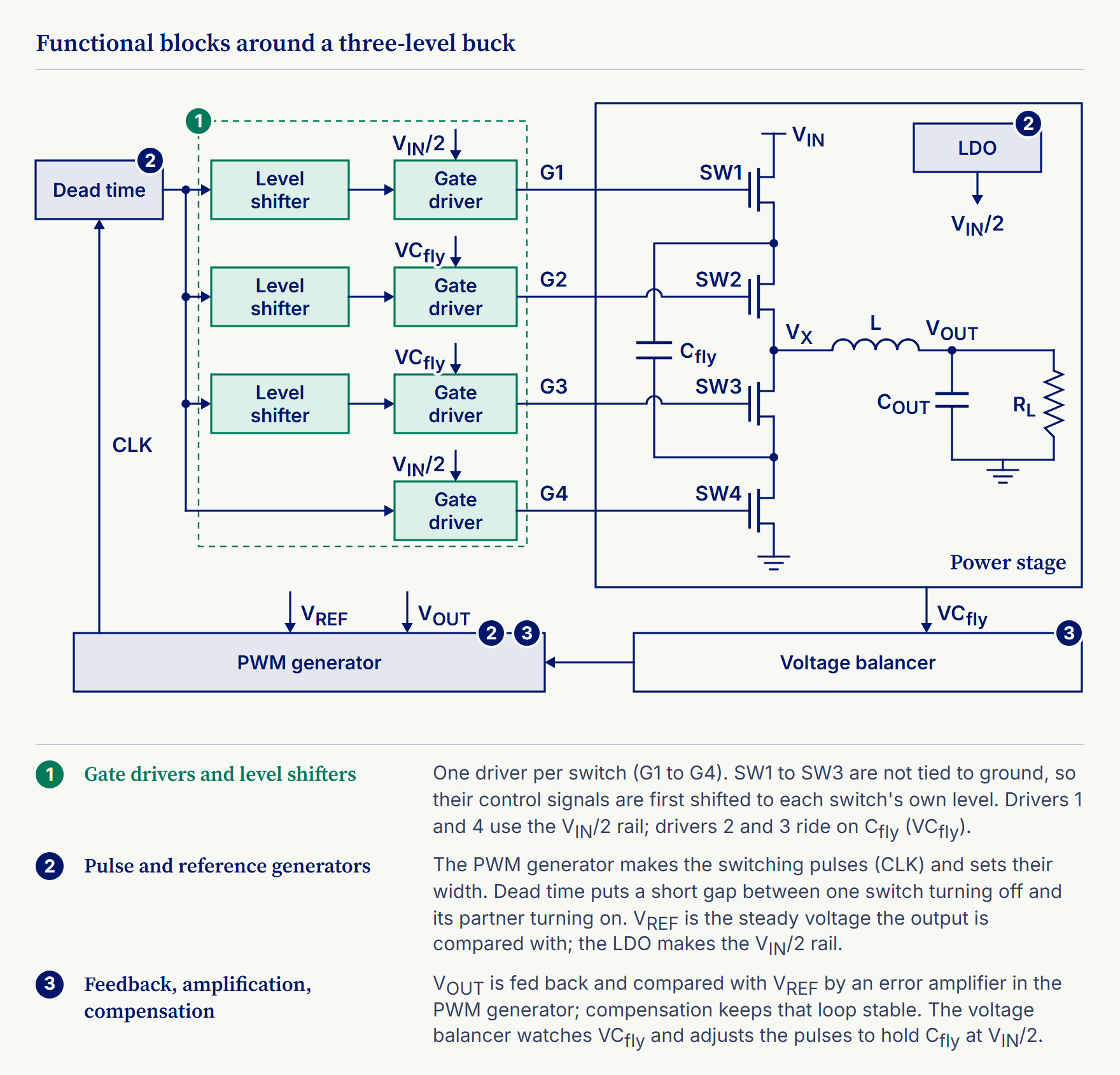
Around a three-level buck the blocks fall into three groups, numbered as in the plate below:
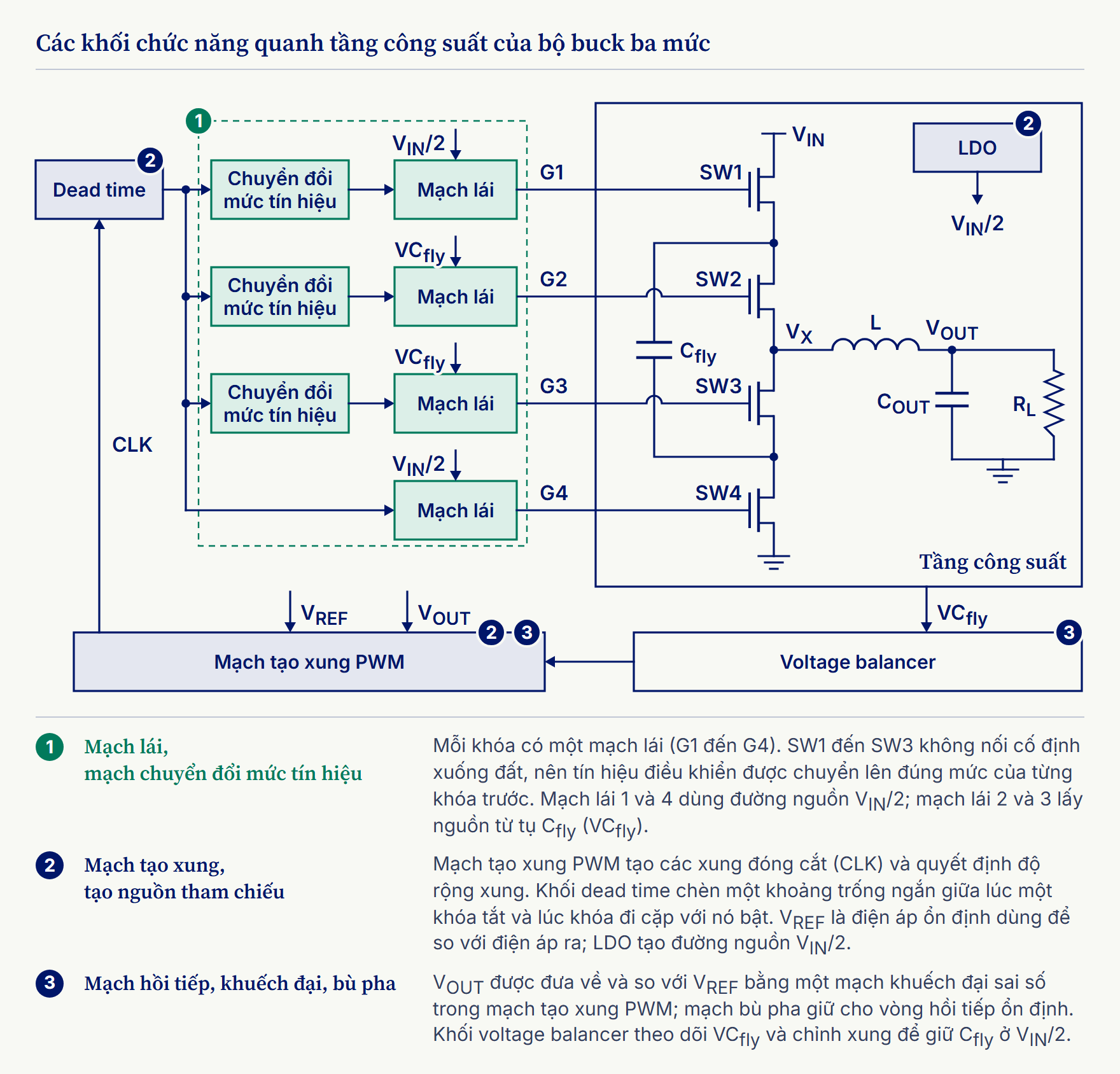
Quanh một bộ buck ba mức, các khối ấy chia thành ba nhóm, đánh số như trong hình dưới đây:
- Gate drivers and level shifters (1). A gate driver turns a weak control signal into the strong, fast pulse that switches a large power transistor, one driver per switch. Three of the four switches are not tied to ground, so a level shifter first moves each one’s control signal to the voltage that switch sits at.
- Pulse and reference generators (2). A pulse-width modulation (PWM) generator makes the train of pulses that times the switches and sets how long each stays on, and a dead-time block leaves a short gap between one switch turning off and the switch paired with it turning on. A voltage reference gives a voltage that barely drifts with temperature or supply, for the output to be compared with.
- Feedback, amplification and compensation (3). The output is fed back and compared with the reference; an amplifier enlarges the difference, which adjusts the pulses, and compensation keeps that loop from oscillating. A voltage balancer holds the flying capacitor at half the input.
- Mạch lái (gate driver) và mạch chuyển đổi mức tín hiệu (level shifter) (1). Mạch lái biến một tín hiệu điều khiển yếu thành xung mạnh và nhanh, đủ sức đóng cắt một transistor công suất lớn; mỗi khóa có một mạch lái riêng. Ba trong bốn khóa không nối đất, nên trước đó mạch chuyển đổi mức phải đưa tín hiệu điều khiển của từng khóa lên đúng mức điện áp của khóa ấy.
- Mạch tạo xung và nguồn tham chiếu (2). Mạch tạo xung PWM (pulse-width modulation) sinh ra chuỗi xung định thời cho các khóa và quyết định mỗi khóa dẫn trong bao lâu, còn khối dead time chèn một khoảng nghỉ ngắn giữa lúc một khóa tắt và lúc khóa đi cặp với nó bật. Nguồn tham chiếu cho một điện áp gần như không trôi theo nhiệt độ hay điện áp nguồn, làm mốc để so với điện áp ra.
- Hồi tiếp, khuếch đại và bù pha (3). Điện áp ra được đưa ngược về để so với nguồn tham chiếu; mạch khuếch đại làm lớn phần chênh lệch để chỉnh lại các xung, còn mạch bù pha giữ cho vòng hồi tiếp ấy không dao động. Khối voltage balancer giữ tụ bay (flying capacitor) ở đúng một nửa điện áp vào.
Each block is built from transistors and checked by simulation
Mỗi khối được dựng từ transistor rồi kiểm tra bằng mô phỏng
Next, each block becomes a circuit. In analog design the smallest element a designer works with is the transistor itself: a gate driver or an amplifier is assembled from individual transistors, capacitors and resistors, drawn as a schematic in a schematic editor, one of the electronic design automation (EDA) tools. This is transistor-level design, the circuit design of step 4 in chapter 2’s flow.
Tiếp theo, mỗi khối trở thành một mạch điện cụ thể. Trong thiết kế analog, người thiết kế làm việc trực tiếp với phần tử nhỏ nhất là chính transistor. Mạch lái hay mạch khuếch đại đều được lắp từ từng transistor, tụ điện và điện trở, rồi được vẽ thành sơ đồ nguyên lý (schematic) trên schematic editor, một công cụ EDA (phần mềm thiết kế chip) dùng để vẽ mạch. Đây là thiết kế mức transistor (transistor-level design), phần thiết kế mạch ở bước 4 trong quy trình của chương 2.
As chapter 2 said, the transistors come from the foundry, in its process design kit (PDK): each device in a library for drawing and simulating, with a SPICE model that tells the simulator how it behaves.5.2, 5.3 What the designer chooses is the size of each transistor: its channel width W and its channel length L, each set on its own; together they give its W/L ratio.
Như chương 2 đã nói, chính foundry, nơi sẽ sản xuất con chip, cung cấp sẵn các transistor trong PDK (bộ tài liệu thiết kế của nhà máy). Mỗi linh kiện nằm trong thư viện dùng để vẽ và mô phỏng, kèm một mô hình SPICE cho trình mô phỏng biết nó hoạt động ra sao.5.2, 5.3 Việc của người thiết kế là chọn kích thước cho từng transistor: chiều rộng kênh W và chiều dài kênh L, mỗi giá trị chọn riêng; hai giá trị ấy cùng cho ra tỷ số W/L.
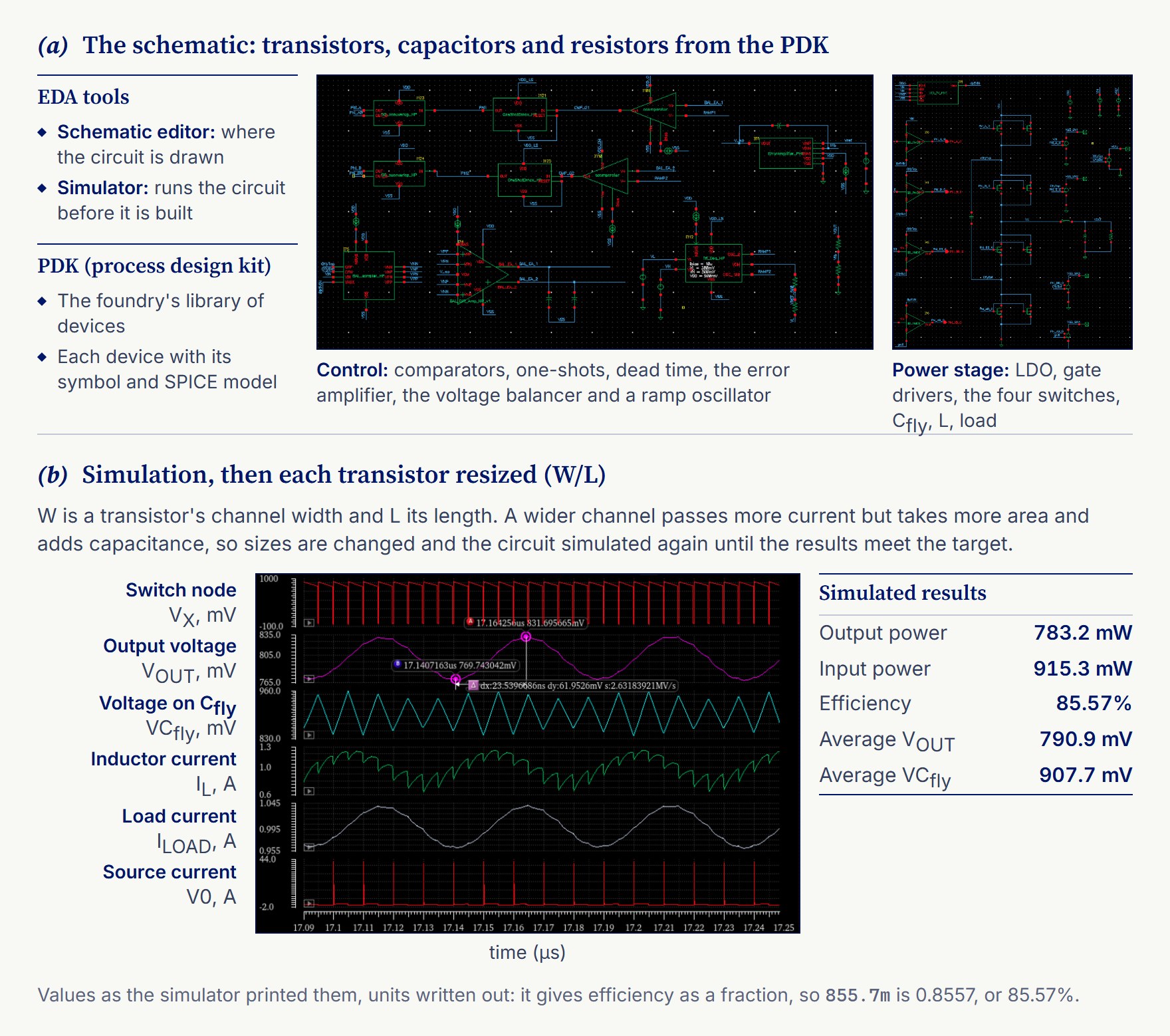
Then comes simulation: the circuit is run in software to see whether each block does its job, whether the amplifier really amplifies, whether the output holds when the load jumps. It is often the step that takes an analog designer the most time, because so much can shift a circuit’s behaviour: the supply voltage, the temperature and the spread of the manufacturing process itself, known together as PVT. The sizes, first worked out on paper, are changed and the circuit simulated again, round after round, until the results meet the target.5.4
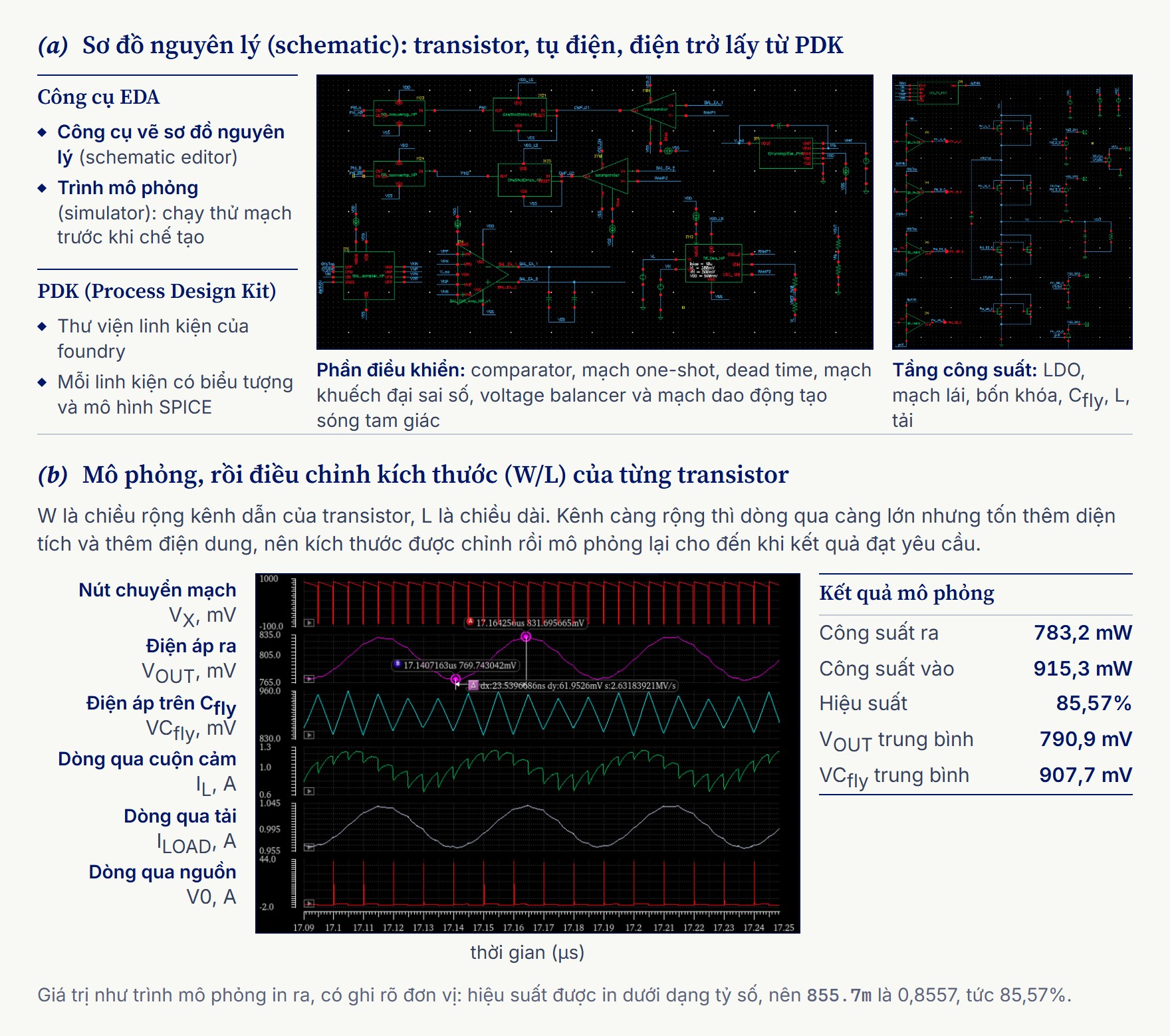
Sau đó là mô phỏng: chạy mạch trên phần mềm để xem từng khối có làm đúng việc của nó không, mạch khuếch đại có thật sự khuếch đại không, điện áp ra có đứng vững khi tải tăng vọt không. Đây thường là bước ngốn nhiều thời gian nhất của người thiết kế analog, vì có quá nhiều yếu tố làm hoạt động của mạch thay đổi: điện áp nguồn, nhiệt độ, và cả sự biến thiên của quy trình sản xuất, gọi chung là PVT (process, voltage, temperature). Kích thước transistor được tính trước trên giấy, rồi chỉnh dần qua từng vòng mô phỏng, hết vòng này đến vòng khác, cho tới khi kết quả đạt mục tiêu.5.4
The plate below shows one such simulation, of a three-level buck from the lab behind this case. The simulator prints efficiency as a fraction: 855.7m means 85.6%, with 0.78 W delivered at 0.79 V, about 1 A.
Hình dưới đây là một lần mô phỏng như thế, trên một bộ buck ba mức của phòng thí nghiệm đứng sau tình huống này. Trình mô phỏng in hiệu suất dưới dạng tỷ số: 855.7m nghĩa là 85,6%, với công suất ra 0,78 W ở 0,79 V, tức khoảng 1 A.
Drawing the layout, checking it and simulating the circuit again
Vẽ layout rồi kiểm tra và mô phỏng lại mạch
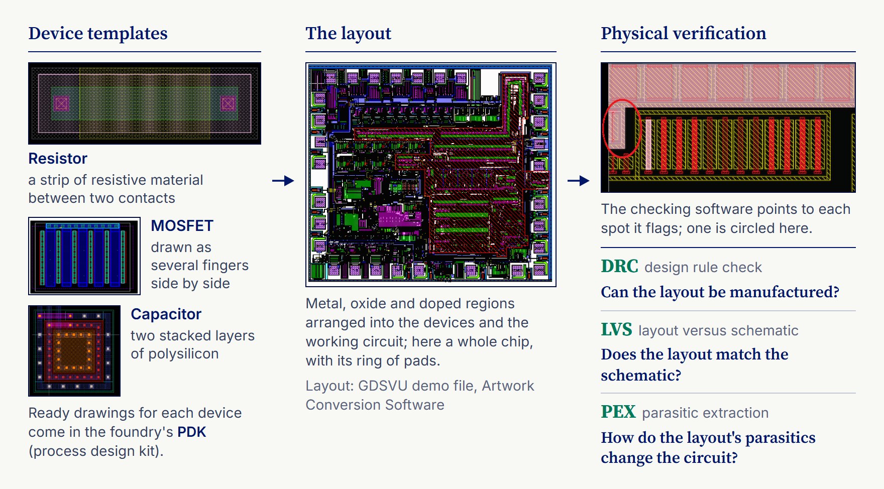
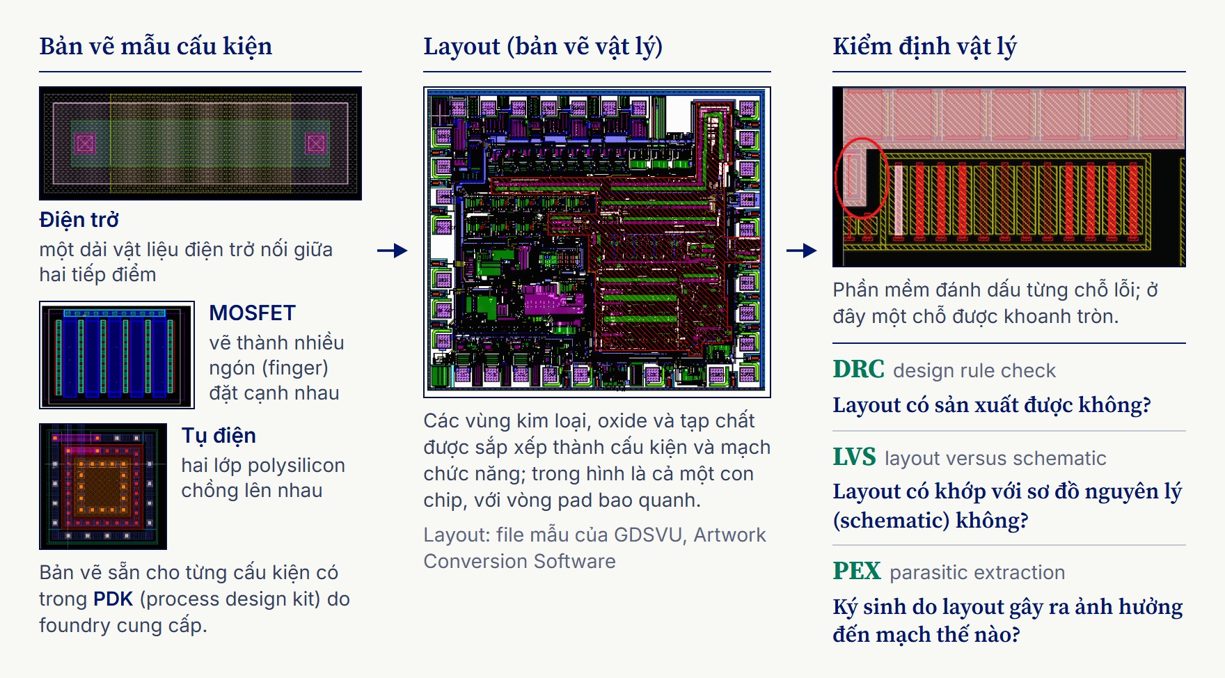
Once the simulations pass, the circuit is drawn as it will exist on silicon. This is physical design, step 5 of the flow, and its product is the layout: the building blocks are now shapes, one set per manufacturing layer, marking where metal, oxide and doped silicon go, so that a transistor becomes a few overlapping rectangles. The PDK supplies a ready drawing for each device, and the designer arranges hundreds of them, with the wires between them, into one complete drawing. The layout is to a chip designer what a finished plan of a house is to an architect: it fixes where everything goes.
Khi các lần mô phỏng đã đạt, người thiết kế vẽ lại mạch đúng như nó sẽ nằm trên silicon. Đó là physical design, bước 5 của quy trình, và sản phẩm của bước này là layout. Lúc này, mạch hiện ra dưới dạng các hình vẽ, mỗi lớp chế tạo một bộ, đánh dấu chỗ nào là kim loại, chỗ nào là oxide, chỗ nào là silicon pha tạp; một transistor chỉ còn là vài hình chữ nhật chồng lên nhau. PDK có sẵn bản vẽ mẫu cho từng linh kiện, và người thiết kế sắp xếp hàng trăm linh kiện như thế, cùng dây nối giữa chúng, thành một bản vẽ hoàn chỉnh. Với người thiết kế chip, layout giống như bản vẽ nhà hoàn thiện với kiến trúc sư: mọi thứ nằm ở đâu đều được chốt trên đó.
Before the layout goes anywhere, software checks it. This is physical verification, step 6: two checks, each answering one question, and beside them a step that extracts what the layout adds to the circuit, so that it can be simulated again:
Trước khi gửi layout đi, phải để phần mềm kiểm tra nó. Đây là khâu kiểm định (verification) dành cho bản vẽ vật lý, gọi là physical verification (bước 6): hai phép kiểm tra, mỗi phép trả lời một câu hỏi, và bên cạnh đó là một bước trích xuất những gì layout thêm vào mạch để mô phỏng lại:
| Step | The question it answers | What it looks at |
|---|---|---|
| DRC, design rule check | Can the layout be manufactured? | every shape, against the foundry’s design rules such as minimum widths and spacings |
| LVS, layout versus schematic | Does the layout match the schematic? | the devices and connections drawn, against the circuit that was simulated |
| PEX, parasitic extraction | How do the layout’s parasitics change the circuit? | the unwanted resistance and capacitance of real wires, put back into the simulation |
| Bước | Câu hỏi cần trả lời | Đối tượng được xét |
|---|---|---|
| DRC (design rule check) | Layout có sản xuất được không? | từng hình vẽ, so với quy tắc thiết kế (design rule) của foundry, như độ rộng và khoảng cách tối thiểu |
| LVS (layout versus schematic) | Layout có khớp với schematic không? | linh kiện và dây nối được vẽ, so với mạch đã mô phỏng |
| PEX (parasitic extraction) | Các thành phần ký sinh do layout tạo ra ảnh hưởng đến mạch thế nào? | điện trở và điện dung không mong muốn của dây nối thật, đưa trở lại vào mô phỏng |
Only when both checks are clean, and the simulations rerun with the extracted parasitics still meet the specification, is the layout ready to be made.5.5, 5.6, 5.7
Chỉ khi cả hai phép kiểm tra đều sạch lỗi, và các lần mô phỏng chạy lại với phần ký sinh đã trích xuất vẫn đạt yêu cầu kỹ thuật, layout mới sẵn sàng đem đi sản xuất.5.5, 5.6, 5.7
Tape-out on a shared wafer
Tape-out trên một wafer dùng chung với nhiều nhóm khác
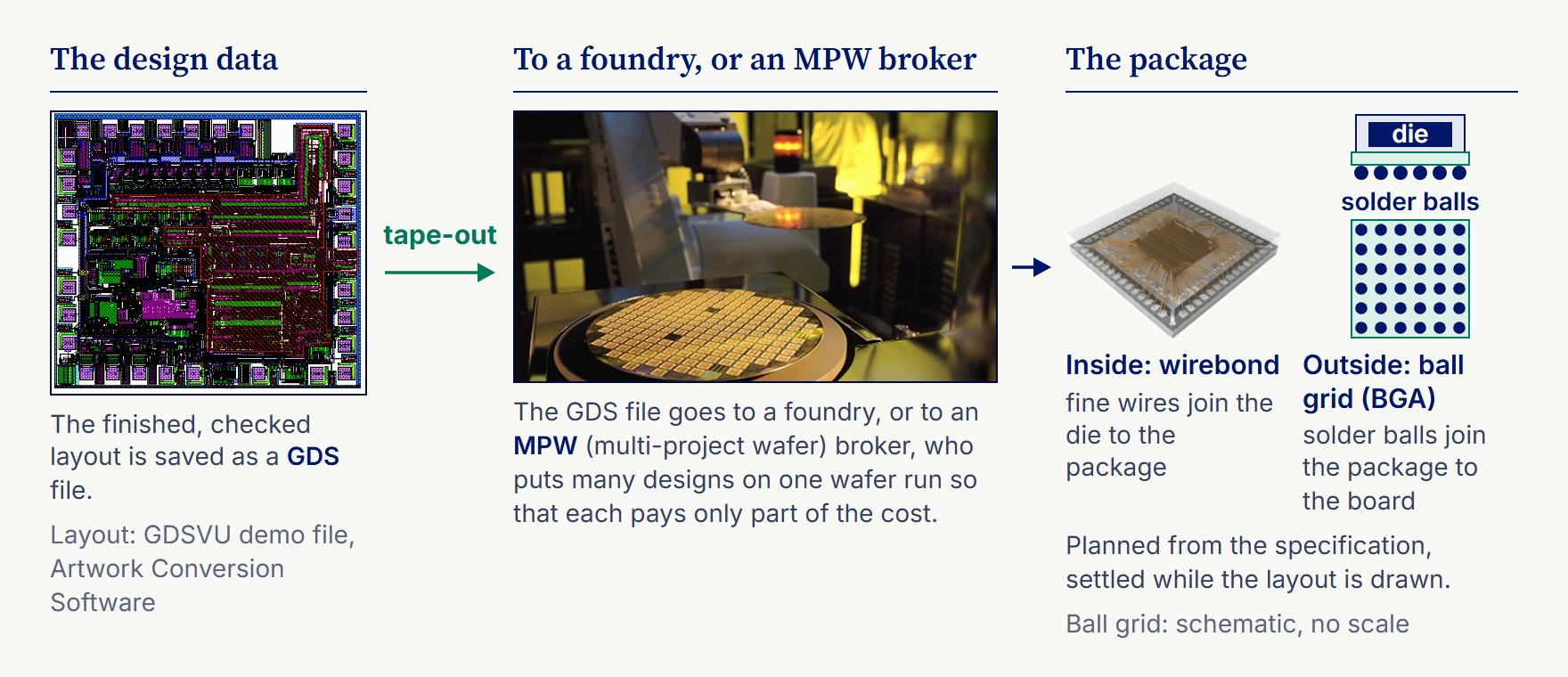
When every check is clean, the finished layout is saved as a GDS file, the standard format for chip drawings, and sent to be made, the hand-over chapter 2 calls tape-out. A company sends its file to a foundry such as TSMC. A university lab rarely pays for a whole wafer run of its own: it sends its GDS file to a multi-project wafer (MPW) broker, who gathers the designs of many groups and companies onto one shared wafer run, so that each pays only part of the cost.5.8, 5.9, 5.10
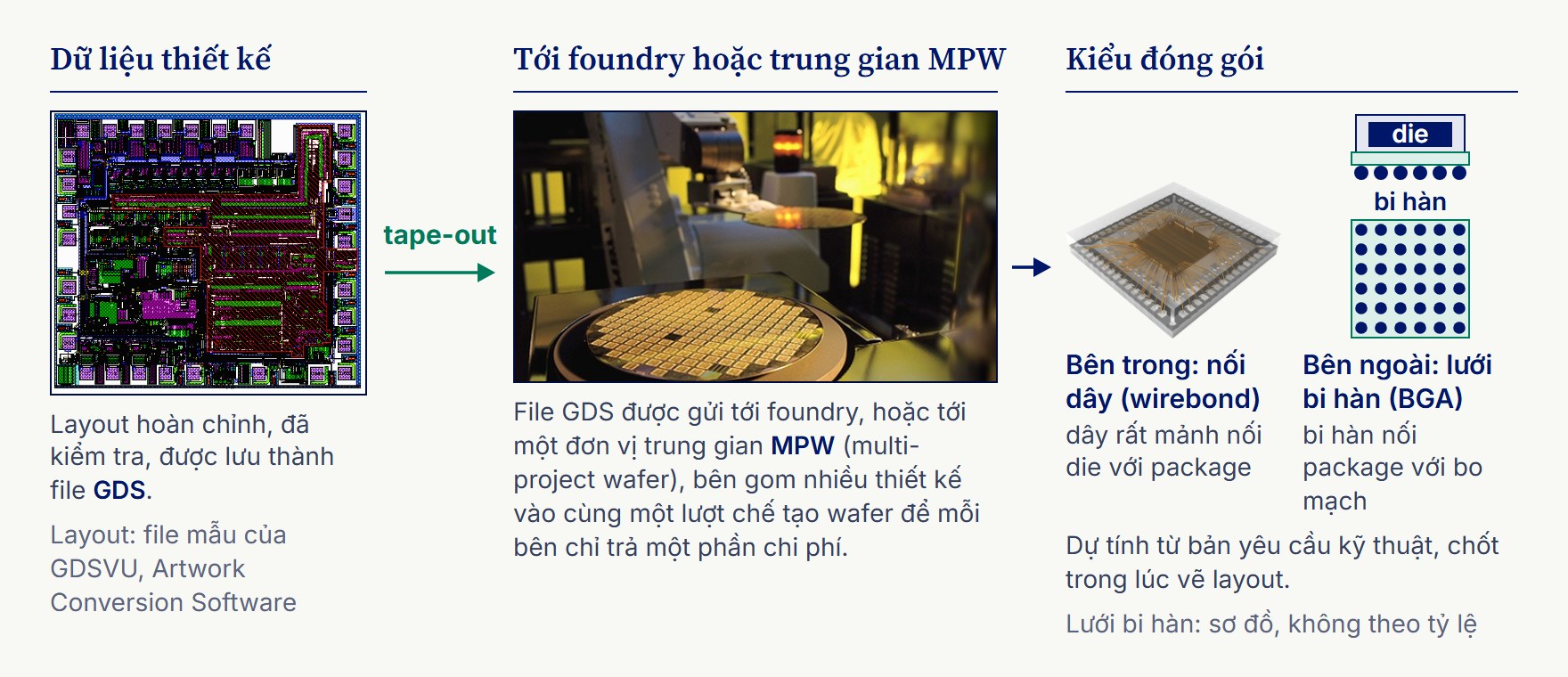
Khi mọi phép kiểm tra đều sạch lỗi, layout hoàn chỉnh được lưu thành file GDS, định dạng chuẩn của bản vẽ chip, rồi gửi đi sản xuất: đó là lần bàn giao mà chương 2 gọi là tape-out. Một công ty gửi file cho foundry, chẳng hạn TSMC. Phòng thí nghiệm đại học thì hiếm khi tự bỏ tiền cho cả một lượt chế tạo wafer riêng. Họ gửi file GDS cho một nhà thầu MPW (wafer dùng chung), bên gom thiết kế của nhiều nhóm và nhiều công ty vào cùng một lượt chế tạo wafer để mỗi bên chỉ trả một phần chi phí.5.8, 5.9, 5.10
The package is planned from the specification and settled while the layout is drawn: chapter 4’s specification named the kinds allowed, and the die’s pads were placed to suit the one chosen. It is designed at two levels. Inside, the die’s pads connect to the package, for example by fine wirebonds; outside, the package connects to the board, by leads along its edges or by a grid of solder balls underneath, a ball grid array (BGA).
Kiểu đóng gói được dự tính ngay từ bản yêu cầu kỹ thuật và chốt trong lúc vẽ layout: bản yêu cầu ở chương 4 đã nêu các kiểu được phép, và layout đặt các pad của die sao cho hợp với kiểu đã chọn. Việc thiết kế package (phần đóng gói của chip) diễn ra ở hai cấp. Bên trong, các pad của die nối với package, chẳng hạn bằng cách nối dây (wirebond), tức dùng những sợi dây rất mảnh; bên ngoài, package nối với bo mạch bằng các chân dọc theo các cạnh hoặc bằng một lưới bi hàn ở mặt dưới, gọi là BGA (ball grid array).
Tape-out ends the design work; the foundry’s mask data preparation (step 7), fabrication (step 8) and packaging and test (step 9) come next. For a university chip it means a wait of a few months while the shared wafers are made, and then the chips come back to the lab.
Tape-out khép lại phần việc thiết kế; tiếp theo là mask data preparation (chuẩn bị dữ liệu mask) của foundry (bước 7), chế tạo (bước 8), rồi đóng gói và kiểm thử (bước 9). Với chip của một trường đại học, điều đó có nghĩa là phải chờ vài tháng cho các tấm wafer dùng chung được sản xuất xong, rồi chip mới về lại phòng thí nghiệm.
The chip comes back and goes onto a test board
Chip trở về và được đưa lên bo mạch thử
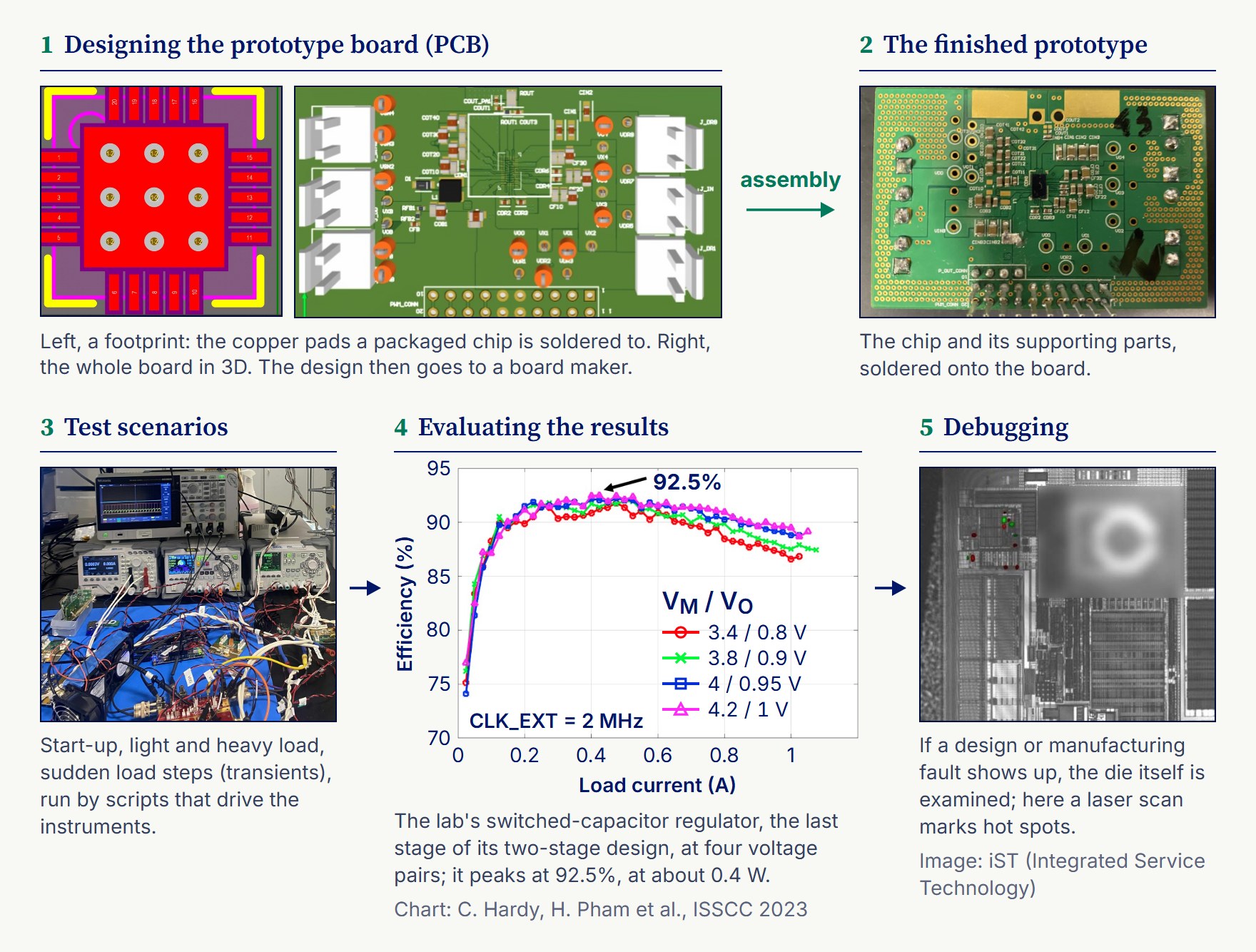
Once the chips are back, the designer’s job turns from drawing to testing. A packaged chip has to sit on a printed circuit board (PCB) before it can be tested on the bench, so the designer, alone or with an application team, designs a test board for it, including the footprint, the pattern of copper pads the chip is soldered to, and sends the design to a board maker. The chip and its supporting parts are then soldered on; in a university lab the students often do that assembly by hand. The result is a prototype board.
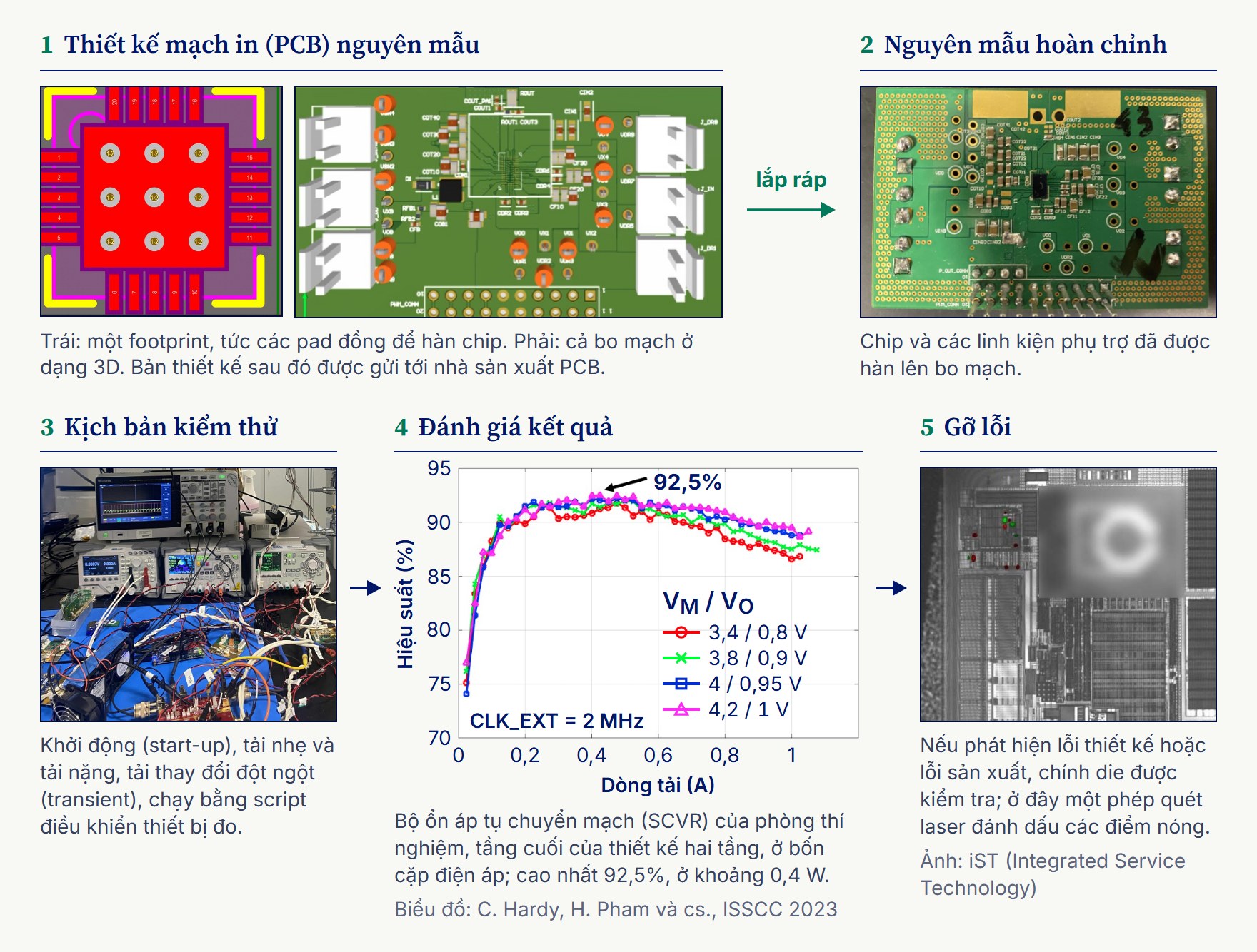
Khi chip đã về, việc của người thiết kế chuyển từ vẽ sang kiểm thử. Một con chip đã đóng gói phải gắn lên mạch in (PCB) mới kiểm thử được trên bàn đo. Vì thế người thiết kế, tự làm hoặc cùng đội thiết kế ứng dụng, thiết kế một bo mạch thử cho nó, kể cả footprint, tức hình mẫu các pad đồng để hàn chip vào, rồi gửi bản thiết kế cho nhà sản xuất mạch in. Sau đó con chip và các linh kiện phụ trợ được hàn lên bo; ở phòng thí nghiệm đại học, sinh viên thường tự tay lắp ráp. Kết quả là một bo mạch nguyên mẫu.
Then comes the bench. The designer writes the test scripts, or helps write them, that drive the lab’s instruments through each case: start-up, light and heavy load, sudden load steps. The results show whether everything designed at the start really works.
Tiếp đến là khâu kiểm thử trên bàn đo. Người thiết kế tự viết, hoặc cùng viết, các kịch bản kiểm thử để điều khiển thiết bị đo trong phòng thí nghiệm qua từng trường hợp: khởi động, tải nhẹ và tải nặng, tải thay đổi đột ngột. Kết quả cho biết mọi thứ thiết kế từ đầu có thật sự chạy đúng hay không.
The plate below shows one such result: the lab’s switched-capacitor regulator, the last stage of the two-stage design in chapter 4, measured at four pairs of input and output voltage.5.11 Its efficiency rises steeply at light load, stays high across the middle of the range and falls off gently at heavy load, peaking at 92.5% at about 0.4 W; as a different circuit from the 10 W worked design, it is not held to that design’s 95% target.
Hình dưới đây là một kết quả như thế, đo trên SCVR (switched-capacitor voltage regulator), bộ ổn áp tụ chuyển mạch của phòng thí nghiệm, ở bốn cặp điện áp vào và ra. Bộ ổn áp này là tầng cuối của thiết kế hai tầng ở chương 4.5.11 Hiệu suất tăng vọt khi tải còn nhẹ, giữ ở mức cao suốt khoảng giữa rồi giảm dần khi tải nặng, cao nhất là 92,5% ở khoảng 0,4 W. Vì là một mạch khác với thiết kế 10 W của ví dụ tính toán, nó không phải đạt mục tiêu 95% của thiết kế ấy.
When something does not work, the fault has to be traced to its cause, a mistake in the design or a defect from manufacturing, and sometimes that means examining the die itself. A failure-analysis lab can scan a die with a laser and mark the hot spots where current leaks; the last step of the plate shows such an image, from a failure-analysis company.
Khi có gì đó không chạy, người ta phải lần ra nguyên nhân, là lỗi thiết kế hay khuyết tật do sản xuất, và đôi khi phải soi tới chính con die. Một phòng thí nghiệm phân tích lỗi (failure analysis) có thể quét die bằng tia laser và đánh dấu những điểm nóng nơi dòng điện rò ra; bước cuối trong hình là một ảnh như thế, của một công ty phân tích lỗi.
Any of these steps may have to be repeated many times, and even a finished chip can still show an error on the bench; what went wrong becomes what the designer does differently next time. In a university lab one student may carry a small chip through every step. On a big team each step has its own owners, and a company’s chip goes further, from its first samples to mass production (chapter 8).
Bước nào trong số này cũng có thể phải làm lại nhiều lần, và ngay cả một con chip đã hoàn chỉnh vẫn có thể lộ lỗi trên bàn đo; cái sai lần này thành bài học cho lần sau. Ở phòng thí nghiệm đại học, một sinh viên có thể tự mình đưa một con chip nhỏ đi qua mọi bước. Trong một đội lớn, mỗi bước có người phụ trách riêng, và chip của doanh nghiệp còn đi xa hơn, từ những mẫu đầu tiên đến sản xuất hàng loạt (chương 8).