Chapter 4 of 10Chương 4/10 11 min11 phút
Flip chip: connecting across the whole faceFlip chip: lật úp con chip để kết nối trên khắp bề mặt
A die joined by wire bonding reaches its package only through the pads along its edge, so its connections grow with its perimeter. Flip chip removes that limit. The die is turned face down and joined to the package through small solder bumps spread across its face, so a connection can sit anywhere on it, each joint only as tall as a bump. The die’s back, now facing up, is left free for the heat to leave through. Many connections, short joints and an open back: that is why processors, graphics chips and AI chips are built this way.
Một die dùng nối dây (wire bonding) chỉ nối ra được với package (phần đóng gói của chip) qua các điểm tiếp xúc (pad) dọc mép, nên số kết nối của nó tăng theo chu vi. Flip chip xóa bỏ giới hạn ấy. Die lật úp xuống, nối với package qua những bump hàn nhỏ trải khắp bề mặt, nên kết nối có thể nằm ở bất cứ đâu trên mặt die, và mỗi mối nối chỉ cao bằng một bump. Mặt lưng của die, giờ quay lên trên, để trống cho nhiệt thoát ra. Nhiều kết nối, mối nối ngắn và mặt lưng để trống: vì thế bộ xử lý, chip đồ họa và chip AI đều dùng cách này.
In this chapter
Trong chương này
- How a die is turned face down and joined across its whole face
- What the bumps, the underfill, the RDL and the lid each do
- Why processors and AI chips use flip chip, and how it differs from wire bonding
- How big a flip-chip package can get
- How several dies and parts share one system-in-package, and how its radios are kept quiet
- Die được lật úp và nối trên khắp bề mặt như thế nào
- Bump, underfill, RDL và nắp, mỗi thứ làm nhiệm vụ gì
- Vì sao bộ xử lý và chip AI dùng flip chip, và flip chip khác nối dây ở những điểm nào
- Một package flip chip có thể lớn đến đâu
- Một system-in-package gom nhiều die và linh kiện ra sao, và được chắn nhiễu thế nào
The die goes face down, and every bump is soldered at once
Die được úp xuống, và mọi bump được hàn cùng một lúc
The die is set face down on the package’s substrate, the small multilayer circuit board under it, and heated until each bump, a small ball of solder on a pad of the die, melts onto a matching pad. Every connection is made at once, instead of one wire at a time.
Die được úp xuống substrate (đế) của package, tức tấm mạch nhỏ nhiều lớp nằm bên dưới, rồi nung nóng cho từng bump, tức một viên hàn nhỏ nằm trên một pad của die, chảy ra và dính vào pad tương ứng. Mọi kết nối hình thành cùng một lúc, thay vì nối từng sợi dây một.
IBM made its first flip chips, transistors joined by solder bumps, in 1962. In a later version, glass dams kept the molten solder from spreading, so the solder alone held the chip up as it melted. That development was named controlled collapse chip connection, or C4, and its bumps were later found safe to place over the whole chip face, not only at its edge.4.1
IBM làm ra những flip chip đầu tiên, các bóng bán dẫn (transistor) nối bằng bump hàn, vào năm 1962. Ở một phiên bản về sau, những gờ thủy tinh giữ cho thiếc hàn nóng chảy không loang ra, nên tự thiếc hàn đỡ được con chip khi chảy. Phương pháp này được đặt tên là controlled collapse chip connection (mối nối chip sụp có kiểm soát), hay C4. Về sau, người ta thấy bump có thể đặt an toàn trên khắp bề mặt chip chứ không chỉ ở mép.4.1
In standard packages the bumps’ pitch, the spacing from one to the next, is about 100 µm and more, ten times closer than the 1.0 mm solder balls common under a package;4.2 Amkor’s flip-chip data sheet lists a minimum of 90 µm.4.3 Chapter 7 sets this rung on its ladder of connection sizes.
Trong các package tiêu chuẩn, pitch (khoảng cách giữa tâm hai tiếp điểm kề nhau) của bump vào khoảng 100 µm trở lên, sát hơn mười lần so với những bi hàn 1,0 mm thường thấy dưới đáy package;4.2 bảng dữ liệu flip chip của Amkor ghi mức nhỏ nhất là 90 µm.4.3 Chương 7 đặt bậc này lên “chiếc thang” kích thước kết nối.
What bumps, underfill and the RDL do
Bump, underfill và RDL làm những việc gì
A flip-chip package has more layers than a wire-bonded one, and each has a job (plate 4.1).
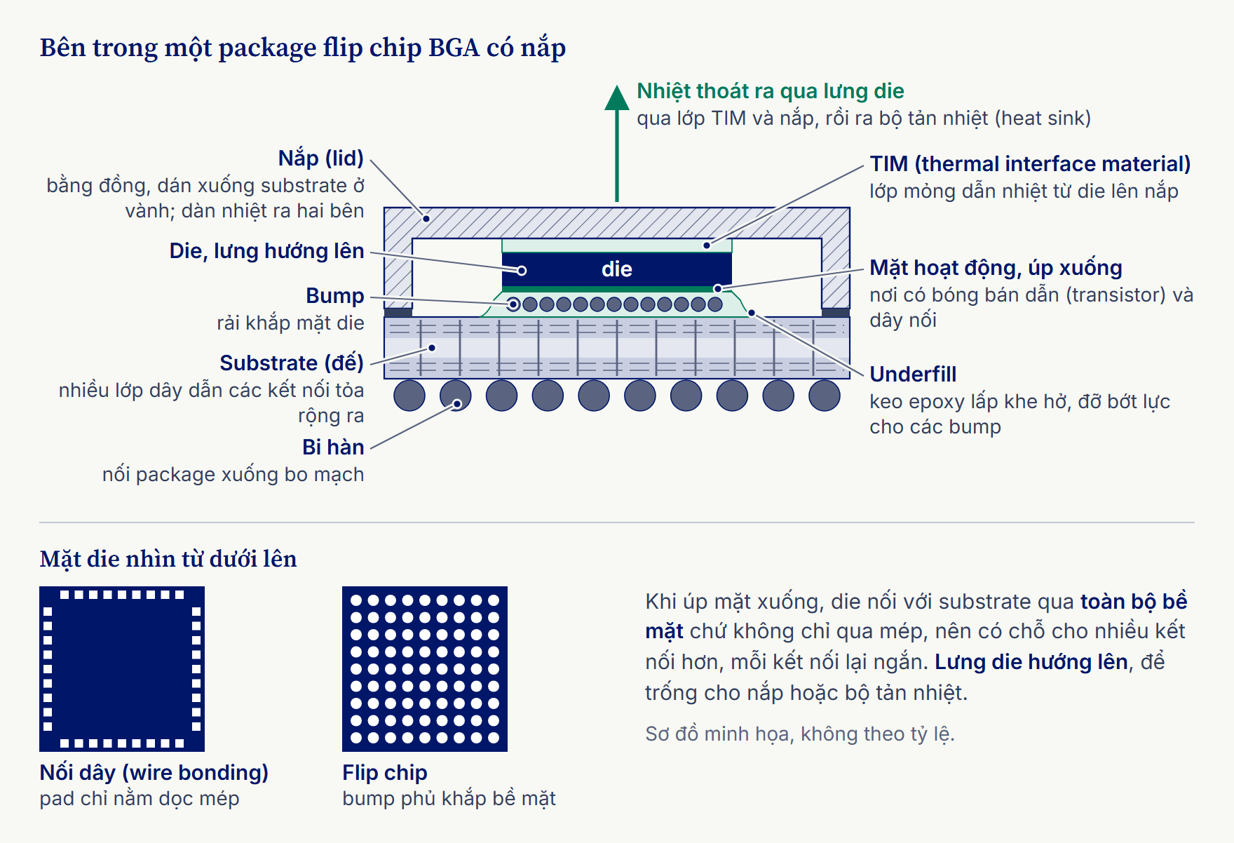
Package flip chip có nhiều lớp hơn package nối dây, và mỗi lớp đảm nhận một việc riêng (hình 4.1).
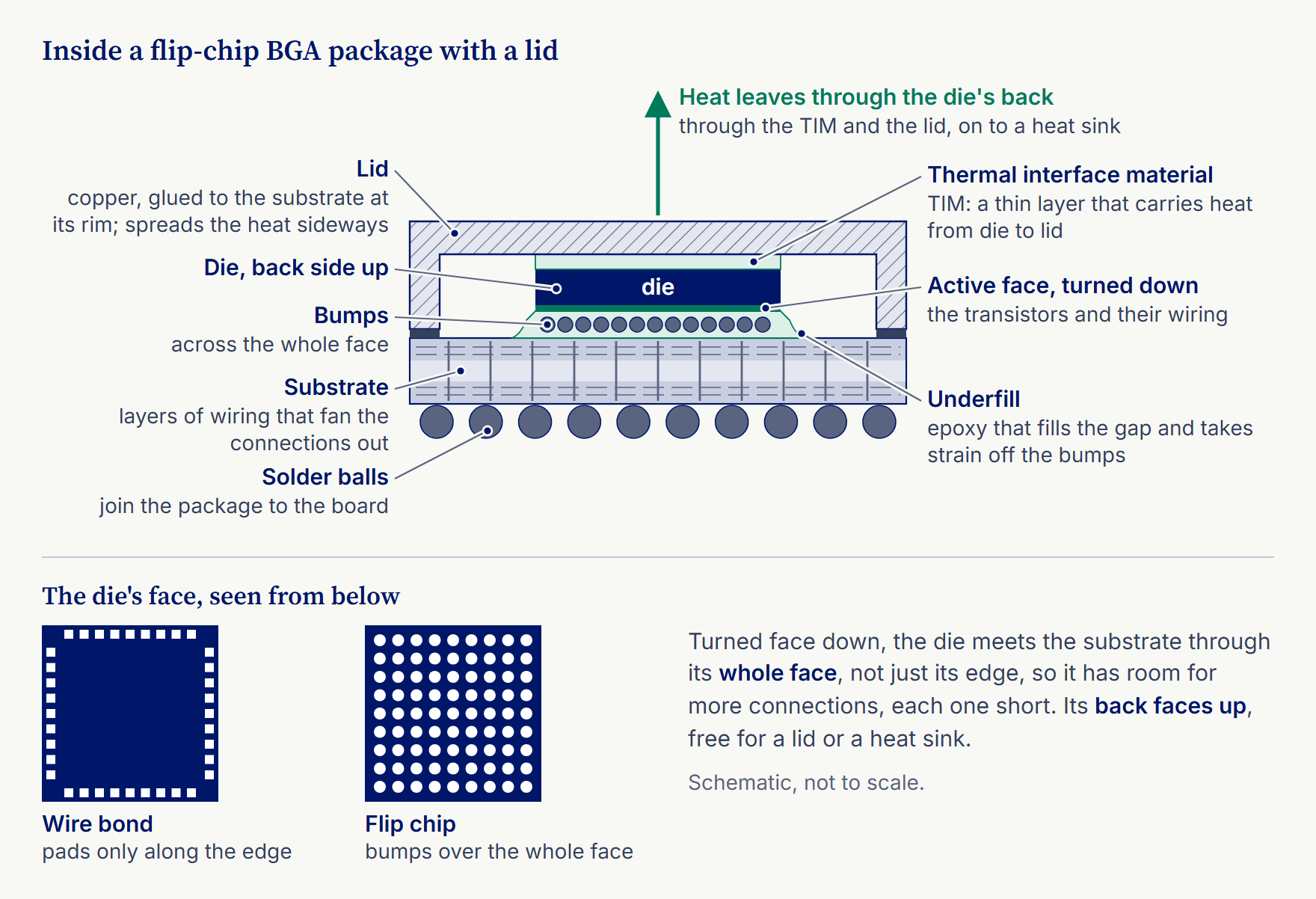
The bumps carry signals and power straight down. Each sits on a thin stack of metals on its pad, the under-bump metallization, which the solder wets and holds to.4.1 A die designed for flip chip has its bump sites spread across its face from the start. Many dies were first laid out with their pads along the edge, for wire bonds; for those, a redistribution layer (RDL), a thin layer of metal wiring added on top of the finished die, moves each pad to a bump site spread across the face.
Bump dẫn tín hiệu và điện năng đi thẳng xuống dưới. Mỗi bump nằm trên một chồng lớp kim loại mỏng phủ trên pad, gọi là under-bump metallization (UBM), để thiếc hàn bám chặt vào.4.1 Die thiết kế cho flip chip có vị trí bump trải khắp bề mặt ngay từ đầu. Còn nhiều die vốn có pad nằm dọc mép để nối dây; với những die ấy, người ta thêm RDL (redistribution layer), tức một lớp dây kim loại mỏng phủ lên die đã hoàn thiện, để dời từng pad tới một vị trí bump trải trên khắp bề mặt.
After soldering, underfill, an epoxy, is flowed into the gap between the die and the substrate. Silicon and the substrate swell by different amounts as they heat and cool, and the underfill holds them together so the strain is spread out instead of cracking the bumps.
Sau khi hàn, người ta bơm underfill (lớp keo lót dưới die), một loại keo epoxy, vào khe giữa die và substrate. Silicon và substrate giãn nở khác nhau khi nóng lên rồi nguội đi, và underfill giữ chúng lại với nhau để ứng suất dàn đều ra thay vì làm nứt bump.
The substrate is usually an organic substrate, a resin board whose layers of wiring fan the bump connections out to the much coarser grid of solder balls underneath, which join the package to the board. A package built this way is a flip-chip ball grid array (FCBGA).
Substrate thường là một organic substrate (đế hữu cơ), tức một tấm bo nhựa có nhiều lớp dây dẫn, dàn các kết nối từ bump ra lưới bi hàn thưa hơn nhiều ở mặt dưới, nơi package được hàn xuống bo mạch. Package làm theo cách này gọi là FCBGA (flip-chip ball grid array).
The die’s back now faces up, and the heat leaves that way: through a thermal interface material (TIM), a thin layer that fills the tiny gaps, into a copper lid that spreads the heat sideways, and on to a heat sink. A wire-bonded die lies the other way up, glued down by its back, so its heat goes down, into the package and the board: a QFN, for one, leaves the metal pad under its die bare, to be soldered to the board as a path for the heat.4.4 What it lacks is a way up to a heat sink.
Mặt lưng của die giờ quay lên trên, và nhiệt thoát ra theo đường ấy: qua TIM (thermal interface material), một lớp vật liệu dẫn nhiệt mỏng lấp đầy những khe hở li ti, sang một nắp đồng giúp tản nhiệt ra xung quanh, rồi tới bộ tản nhiệt. Die nối dây thì nằm ngược lại, mặt lưng dán xuống dưới, nên nhiệt đi xuống package và bo mạch: chẳng hạn, package QFN để lộ phần pad kim loại dưới die, hàn thẳng xuống bo mạch làm đường thoát nhiệt.4.4 Điều nó thiếu là một lối thoát lên phía trên, tới bộ tản nhiệt.
Why processors and AI chips use flip chip
Vì sao bộ xử lý và chip AI dùng flip chip
For high-performance CPUs, GPUs and AI chips, flip chip has become all but the only choice, for four reasons. First, these chips need far more connections, for signals and for power, than their edges can hold, and flip chip uses the whole face. Second, the paths are short, so each connection adds little of the parasitic inductance that slows fast signals and lets the supply voltage dip when the current jumps. Third, the heat leaves through the exposed back, and these chips run hot. Fourth, with every connection under the die, several dies can sit close together on one substrate: a processor beside its memory, or a large die on the newest node beside smaller ones made on older, cheaper nodes, which chapter 6 takes further.
Với các CPU, GPU và chip AI hiệu năng cao, flip chip gần như là lựa chọn duy nhất, vì bốn lẽ. Thứ nhất, những con chip này cần nhiều kết nối cho tín hiệu và nguồn điện hơn hẳn số mà mép của chúng chứa được, còn flip chip dùng cả bề mặt. Thứ hai, đường nối ngắn, nên mỗi kết nối chỉ thêm rất ít điện cảm ký sinh, thứ làm chậm tín hiệu tốc độ cao và khiến điện áp nguồn bị sụt khi dòng điện tăng vọt. Thứ ba, nhiệt thoát qua mặt lưng để trống, mà những con chip này lại rất nóng. Thứ tư, khi mọi kết nối đều nằm ngay dưới die, nhiều die có thể đặt sát nhau trên cùng một substrate. Có thể là bộ xử lý nằm cạnh bộ nhớ của nó, hoặc một die lớn ở tiến trình bán dẫn (technology node) mới nhất nằm cạnh những die nhỏ ở tiến trình cũ, rẻ hơn. Chương 6 bàn tiếp hướng này.
Inductance is where the two methods differ most sharply. It resists any quick change in current, and a wire has far more of it than a bump.
Hai phương pháp khác nhau rõ nhất ở điện cảm. Điện cảm cản trở mọi thay đổi nhanh của dòng điện, và một sợi dây có điện cảm lớn hơn nhiều so với một bump.
| Wire bond against flip chip | Wire bond | Flip chip |
|---|---|---|
| Where the contacts sit | Pads along the die’s edge only | Bumps across the whole face of the die |
| The path a connection takes | Up from the pad, over a loop of wire measured in millimetres, down to the package | Straight down through one bump into the substrate |
| Inductance | About 1 nH for each millimetre of wire4.5 | As little as about 50 pH for a bump4.5 |
| How the heat leaves | Die face up, glued down by its back: heat goes down through the die attach into the board, best through a bare metal pad soldered to it; no way up to a heat sink4.4 | Die back up: heat goes straight out through a TIM, a lid and a heat sink |
| Cost | The proven, cheaper choice for chips with fewer and slower connections | Bumping the die and a finer substrate cost more; worth it when a chip needs many fast connections |
| Nối dây và flip chip | Nối dây | Flip chip |
|---|---|---|
| Tiếp điểm nằm ở đâu | Chỉ có pad dọc mép die | Bump trải khắp bề mặt die |
| Đường đi của một kết nối | Từ pad đi lên, vòng qua một sợi dây dài cỡ milimet, rồi xuống package | Đi thẳng xuống qua một bump vào substrate |
| Điện cảm | Khoảng 1 nH cho mỗi milimet dây4.5 | Chỉ khoảng 50 pH cho một bump4.5 |
| Nhiệt thoát ra thế nào | Die ngửa mặt, lưng dán xuống dưới: nhiệt đi xuống qua lớp keo gắn die vào bo mạch, tốt nhất qua một pad kim loại để lộ, hàn thẳng xuống bo; không có lối lên bộ tản nhiệt4.4 | Lưng die quay lên: nhiệt thoát thẳng qua TIM, nắp và bộ tản nhiệt |
| Chi phí | Lựa chọn đã được kiểm chứng và rẻ hơn cho chip cần ít kết nối, tốc độ thấp hơn | Tạo bump trên die và substrate mịn hơn khiến giá cao hơn; đáng đồng tiền khi chip cần nhiều kết nối tốc độ cao |
How big a flip-chip package gets
Một package flip chip có thể lớn đến đâu
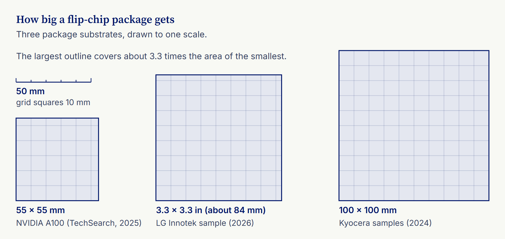
As chips grew and packages began to carry several dies, flip-chip packages grew with them. Three package substrates, drawn to one scale in plate 4.2, show how large they get: the 55 × 55 mm substrate under NVIDIA’s A100, whose dies sit on a silicon interposer (chapter 6), as an analyst’s 2025 survey of AI packages lists it;4.6 a sample about 84 mm a side (3.3 inches) that LG Innotek showed in 2026;4.7 and the 100 × 100 mm substrates Kyocera offered as samples in 2024.4.8 The largest covers about 3.3 times the area of the smallest. For an older reference point, Amkor’s FCBGA data sheet (Rev 12/20) lists bodies from 10 mm to 67.5 mm on a side, with an 85 mm body in development.4.3
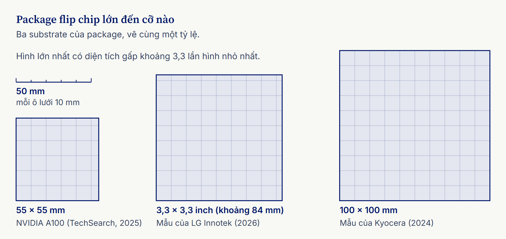
Chip càng lớn và package càng chứa nhiều die thì package flip chip cũng lớn theo. Ba substrate của package, vẽ cùng một tỷ lệ ở hình 4.2, cho thấy package có thể lớn đến mức nào: substrate 55 × 55 mm dưới chip A100 của NVIDIA, nơi các die nằm trên một silicon interposer (chương 6), theo khảo sát năm 2025 của một hãng phân tích về các package cho AI;4.6 một mẫu khoảng 84 mm mỗi cạnh (3,3 inch) mà LG Innotek giới thiệu năm 2026;4.7 và các substrate 100 × 100 mm mà Kyocera chào hàng dưới dạng mẫu năm 2024.4.8 Cỡ lớn nhất có diện tích gấp khoảng 3,3 lần cỡ nhỏ nhất. Để đối chiếu với một mốc cũ hơn, bảng dữ liệu FCBGA của Amkor (bản 12/2020) liệt kê các thân package từ 10 mm đến 67,5 mm mỗi cạnh, và một cỡ 85 mm đang được phát triển.4.3
A system-in-package holds many parts on one substrate
Một system-in-package gom nhiều linh kiện trên cùng một substrate
A system-in-package (SiP) uses one substrate to hold several dies and parts that would otherwise sit apart on a board. The dies may be joined in different ways, some by flip chip and some by wire bonding, and some may go in already packaged. Beside them sit passive components such as capacitors and inductors that steady their power, and often all of it is sealed under one layer of molding compound (plate 4.3). The whole module then goes onto the board as one part.
System in Package (SiP) dùng một substrate để chứa nhiều die và linh kiện mà lẽ ra phải nằm rải rác trên bo mạch. Các die có thể được nối theo nhiều cách: có die nối bằng flip chip, có die nối dây, và có die được đưa vào khi đã đóng gói sẵn. Bên cạnh là các passive component (linh kiện thụ động) như tụ điện và cuộn cảm giúp ổn định nguồn điện, và thường thì tất cả nằm chung dưới một lớp nhựa bọc (hình 4.3). Sau đó cả module gắn lên bo mạch như một linh kiện duy nhất.
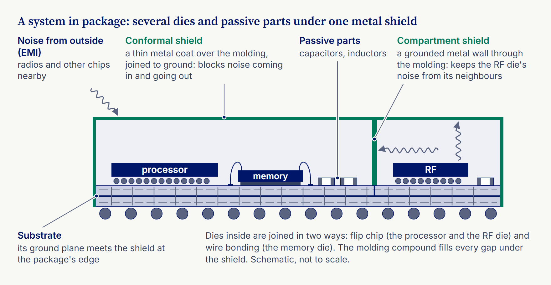
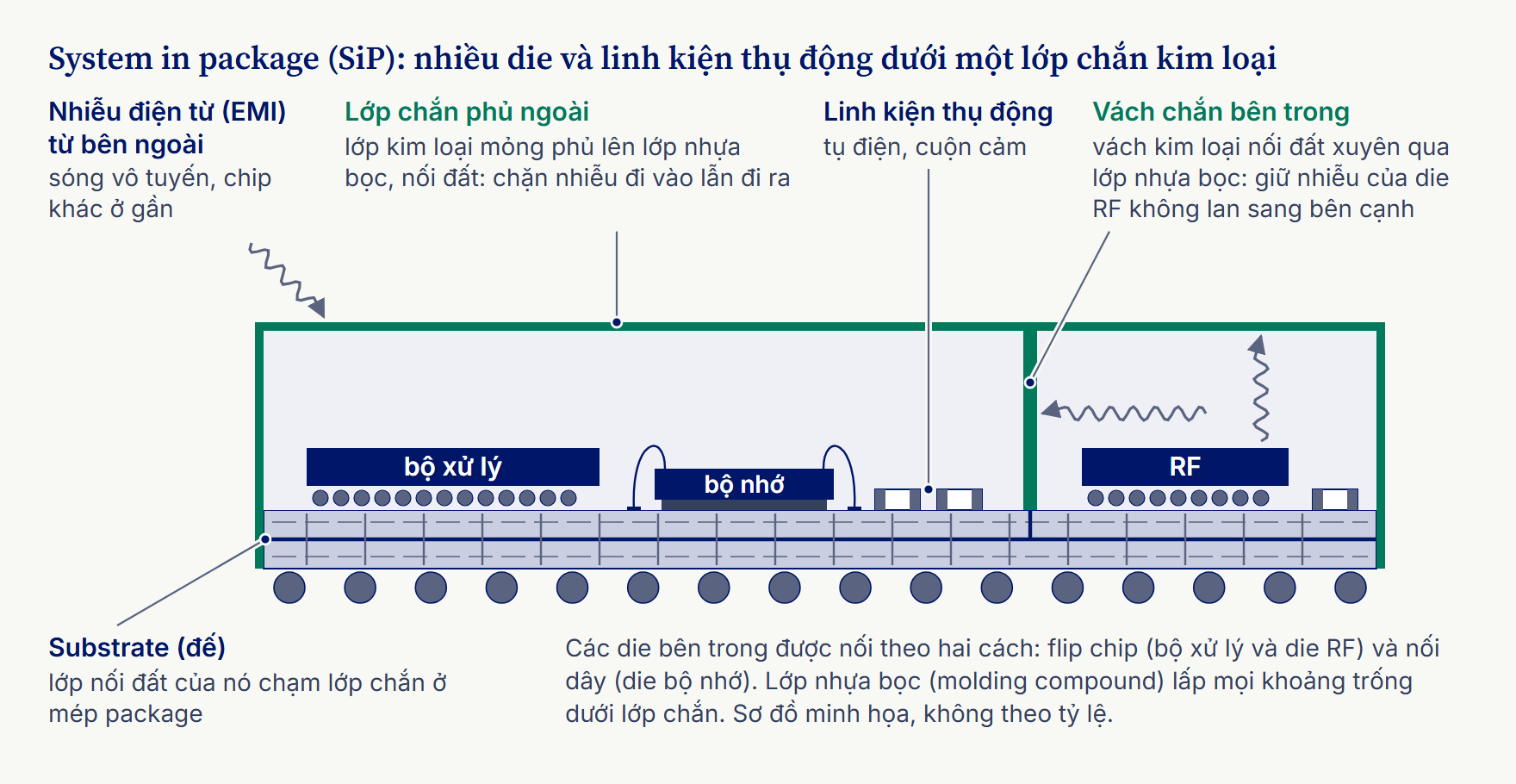
Packing radios and processors this close brings a problem: electromagnetic interference (EMI), noise sent out by one circuit and picked up by another. The older shielding was a metal can or lid fitted over the module. ASE describes what replaced it: a thin metal film deposited over the whole package and joined to ground (conformal shielding), and inside it, sensitive parts walled off by a trench cut with a laser and filled with conductive paste (compartment shielding).4.9 ASE reports that dropping the can made its modules 17% smaller in area and 7% thinner.
Khi các mạch vô tuyến và bộ xử lý nằm sát nhau như vậy, một vấn đề nảy sinh: electromagnetic interference (EMI), tức nhiễu điện từ do một mạch phát ra và mạch khác thu phải. Cách EMI shielding (lớp chắn nhiễu điện từ) trước đây là chụp một hộp hoặc nắp kim loại lên module. ASE mô tả cách làm đã thay chiếc hộp ấy: bên ngoài, một màng kim loại mỏng phủ lên toàn bộ package và nối đất (conformal shielding); bên trong, những phần nhạy cảm được ngăn riêng bằng một rãnh cắt laser, lấp đầy keo dẫn điện (compartment shielding).4.9 Theo ASE, bỏ được hộp kim loại giúp module của hãng nhỏ hơn 17% về diện tích và mỏng hơn 7%.
Flip chip still joins its dies to a substrate whose wiring is coarse next to the die’s own. Chapter 5 builds packages on the wafer itself, and chapter 6 sets dies side by side on finer wiring of silicon.
Dù vậy, flip chip vẫn nối die với một substrate có dây dẫn thô hơn nhiều so với dây dẫn trên chính die. Chương 5 đóng gói chip ngay trên wafer, còn chương 6 đặt các die cạnh nhau trên lớp dây dẫn mịn hơn làm bằng silicon.
Does flip chip give more bandwidth than wire bonding?Flip chip có cho băng thông cao hơn nối dây không?
Bandwidth depends on how many connections a chip has and how fast each one can carry data, and flip chip helps both. The gain per connection is usually stated as inductance, not as gigabits per second (the table above gives the figures). The smaller the inductance, the sharper the edges a signal keeps and the less the supply voltage sags when many circuits switch at once, so a bump can carry faster signals than a comparable wire.
Băng thông phụ thuộc vào số kết nối của con chip và tốc độ truyền dữ liệu của từng kết nối, và flip chip có lợi ở cả hai mặt. Lợi thế trên mỗi kết nối thường được nêu bằng điện cảm chứ không bằng gigabit mỗi giây (con số nằm ở bảng trên). Điện cảm càng nhỏ thì sườn tín hiệu càng giữ được độ dốc và điện áp nguồn càng ít bị sụt khi nhiều mạch chuyển mạch cùng lúc, nên bump truyền được tín hiệu nhanh hơn một sợi dây tương đương.
Does the RDL slow a chip's I/O down?Lớp RDL có làm chậm tín hiệu vào ra của chip không?
Not necessarily: it depends on how long and how fine its wires are. An RDL’s wires are short, and a package wired with RDL instead of a substrate can even be faster: TSMC reports that its InFO_PoP, built on RDL with no organic substrate and no C4 bumps, performs better electrically than a flip-chip package-on-package (chapter 5).4.10 Finer wires do have more resistance. One simulation study (Georgia Tech, IEEE ICCD 2020) compared a 2.5D design built on a silicon interposer, a thin layer of fine wiring that several dies sit on (chapter 6), with the same design on an organic interposer whose wires are fatter. The organic interposer’s worst wire delay was 0.75 times the silicon one’s, because fatter wires have less resistance, but the height of the “eye” a receiver sees, the opening between a one and a zero, was about 22% lower: with so little resistance, reflections of the signal died away more slowly and blurred the bits.4.11
Không hẳn: điều đó tùy dây dẫn của nó dài và mảnh đến đâu. Dây của RDL ngắn, và một package đi dây bằng RDL thay cho substrate còn có thể nhanh hơn: theo TSMC, InFO_PoP của hãng, dựng trên RDL, không có substrate hữu cơ và bump C4, có hiệu năng điện tốt hơn PoP dùng flip chip (chương 5).4.10 Dù vậy, dây càng mảnh thì điện trở càng lớn. Một nghiên cứu mô phỏng (Georgia Tech, IEEE ICCD 2020) so sánh một thiết kế 2.5D đặt trên silicon interposer, tức một lớp dây dẫn mịn mà nhiều die cùng nằm lên (chương 6), với chính thiết kế ấy trên một interposer hữu cơ có dây to hơn. Độ trễ lớn nhất trên các dây của interposer hữu cơ chỉ bằng 0,75 lần của silicon interposer, vì dây to có điện trở nhỏ hơn, nhưng độ cao của “mắt tín hiệu” mà bộ thu nhìn thấy, tức khoảng mở giữa bit 1 và bit 0, thấp hơn khoảng 22%: điện trở nhỏ khiến tín hiệu phản xạ tắt chậm hơn và làm nhòe các bit.4.11
What holds packaging back at the most advanced nodes?Ở những tiến trình tiên tiến nhất, điều gì cản trở khâu đóng gói chip?
One well-documented limit is stress where the package meets the chip. An advanced chip’s top wiring layers are insulated with low-k materials, chosen because they store less charge between neighbouring wires, and these are often porous and mechanically weak. In fine-pitch flip-chip packages with hard copper pillars in place of round bumps, the stress the package puts on those layers as it heats and cools can make them crack or peel apart, a problem called chip-package interaction. A 2025 study notes that a low-k layer has a higher risk of cracking than an oxide layer, and looks at how the design of the wiring layers changes that risk.4.12
Một giới hạn đã được ghi nhận rõ là ứng suất ở chỗ package tiếp giáp với con chip. Các lớp dây dẫn phía trên của một con chip tiên tiến dùng vật liệu low-k để cách điện, loại vật liệu người ta chọn vì tích ít điện tích giữa hai dây nằm cạnh nhau, nhưng thường xốp và yếu về cơ học. Trong các package flip chip pitch nhỏ dùng trụ đồng cứng thay cho bump tròn, ứng suất mà package dồn lên những lớp này khi nóng lên rồi nguội đi có thể làm chúng nứt hoặc bong tách, hiện tượng gọi là tương tác giữa chip và package (chip-package interaction). Một nghiên cứu năm 2025 chỉ ra rằng lớp low-k có nguy cơ nứt cao hơn lớp oxit, và xem xét cách thiết kế các lớp dây dẫn làm thay đổi nguy cơ ấy.4.12