Chapter 7 of 10Chương 7/10 10 min10 phút
Stacking chips: memory towers and copper bondsXếp chồng chip: từ tháp bộ nhớ đến mối nối đồng với đồng
Chips set side by side, as on an interposer, a thin base wired to link them, talk mostly through the edges that face each other. Stack one die, a piece of silicon cut from a wafer, on top of another, and the two can connect across the whole face they share. In AI chips, memory was stacked first: the largest AI processors are ringed by towers of memory dies called high-bandwidth memory (HBM).
Khi đặt cạnh nhau, chẳng hạn trên một interposer, tức tấm nền mỏng có dây dẫn nối các chip với nhau, các chip chủ yếu trao đổi tín hiệu qua phần mép đối diện nhau. Nếu xếp một die (mảnh silicon cắt ra từ wafer) chồng lên một die khác, hai die có thể nối với nhau trên toàn bộ mặt tiếp giáp. Trong chip AI, bộ nhớ là thứ được xếp chồng trước tiên: quanh những bộ xử lý AI lớn nhất là các tháp die nhớ gọi là bộ nhớ băng thông cao (high-bandwidth memory, HBM).
Quick questionThử đoán xem
How many DRAM dies are stacked in each HBM4 stack of NVIDIA's Rubin GPU?Mỗi chồng HBM4 trên GPU Rubin của NVIDIA gồm bao nhiêu die DRAM xếp chồng lên nhau?
Show the answerXem đáp án
Twelve. NVIDIA’s Rubin GPU carries up to 288 GB of HBM4, the sixth generation of HBM, in stacks of 12 DRAM dies, the working memory a processor reads and writes all the time.7.1, 7.2 The HBM4 standard allows stacks of 4, 8, 12 or 16 dies (as reported, TrendForce, April 2025),7.3 and SK hynix showed a 16-high, 48 GB part in January 2026,7.4 but Rubin’s stacks are 12 high.
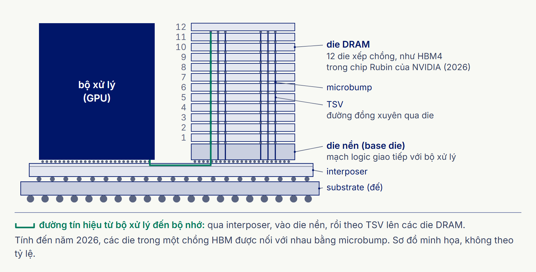
Mười hai. GPU Rubin của NVIDIA mang tối đa 288 GB HBM4, thế hệ thứ sáu của HBM, xếp thành các chồng gồm 12 die DRAM, loại bộ nhớ làm việc mà bộ xử lý đọc và ghi liên tục.7.1, 7.2 Chuẩn HBM4 cho phép mỗi chồng có 4, 8, 12 hoặc 16 die (theo TrendForce, tháng 4/2025),7.3 và SK hynix đã giới thiệu loại chồng 16 die, dung lượng 48 GB, vào tháng 1/2026,7.4 nhưng mỗi chồng trên Rubin chỉ cao 12 die.
In this chapter
Trong chương này
- How memory dies are stacked into a tower
- How two dies are bonded copper straight to copper
- How many more connections fit in the same square at each step
- Which company offers which stacking platform
- Why chips are still set side by side
- Các die nhớ được xếp chồng thành tháp ra sao
- Hai die được nối thẳng đồng với đồng như thế nào
- Ở mỗi nấc thang, cùng một ô vuông chứa thêm bao nhiêu kết nối
- Hãng nào cung cấp nền tảng xếp chồng die nào
- Vì sao chip vẫn được đặt cạnh nhau
How HBM stacks memory into a tower
HBM xếp chồng các die nhớ thành tháp như thế nào
An AI processor needs huge amounts of data every second, so its memory has to sit close and deliver a great deal at once. HBM does it by stacking. A tower of DRAM dies stands on a base die, logic that talks to the processor, and the whole stack sits beside the processor on the interposer. Signals climb the tower through TSVs (through-silicon vias), copper paths that run straight through each die. The dies are joined by microbumps, very small bumps, often copper pillars with a solder cap, set a few tens of micrometres apart; they carry signals and power between the dies, and the same kind join chips to an interposer in chapter 6.
Bộ xử lý AI cần một lượng dữ liệu khổng lồ mỗi giây, nên bộ nhớ phải nằm thật gần và cấp được thật nhiều dữ liệu cùng lúc. HBM làm được điều đó nhờ xếp chồng. Một tháp die DRAM đứng trên một die nền, phần mạch logic giao tiếp với bộ xử lý, và cả chồng được đặt cạnh bộ xử lý trên interposer. Tín hiệu đi lên tháp qua các TSV (through-silicon via), những đường đồng chạy thẳng xuyên qua từng die. Các die nối với nhau bằng microbump, những bump rất nhỏ, thường là trụ đồng có mũ thiếc hàn, cách nhau vài chục micromet, đóng vai trò liên kết điện (interconnect), mang tín hiệu và điện năng giữa các die; đây cũng là loại bump dùng để gắn chip lên interposer ở chương 6.
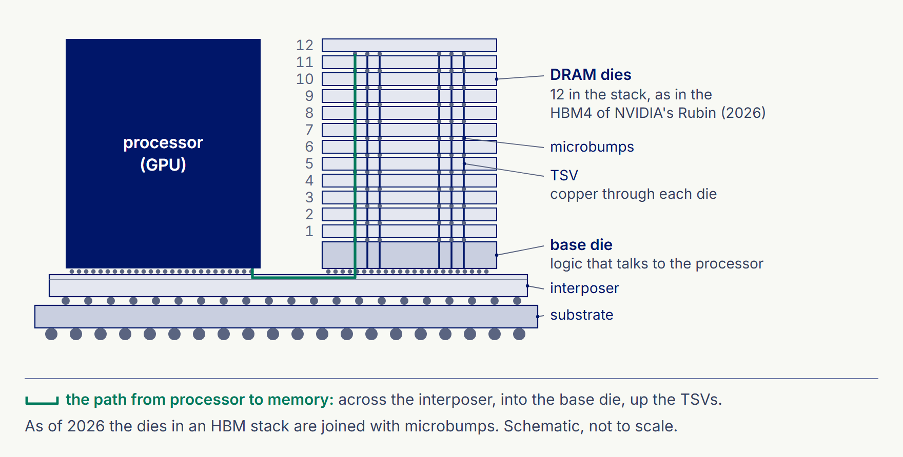
HBM has been in products for about a decade. AMD launched the Radeon R9 Fury X in June 2015, the world’s first graphics family with HBM in AMD’s own words.7.5
HBM đã có mặt trong sản phẩm khoảng mười năm. Tháng 6/2015, AMD ra mắt card đồ họa Radeon R9 Fury X, theo lời AMD là dòng card đồ họa đầu tiên trên thế giới dùng HBM.7.5
SK hynix and Samsung each described their method for the HBM3E generation (2024). In SK hynix’s method, the dies are stacked, all their joints are soldered in one pass of heat, then a liquid protective material is injected between them and hardened, an underfill for the whole stack; SK hynix calls it MR-MUF, mass reflow molded underfill.7.6 In Samsung’s, a non-conductive film is laid between the dies and they are pressed together under heat; Samsung calls it TC NCF, thermal compression with non-conductive film, and it kept Samsung’s 12-high HBM3E as low as an 8-high part.7.7 Hybrid bonding, the solder-free method of the next section, is likely to reach HBM no earlier than 16-high HBM4E, as reported (TrendForce, July 2026, citing industry forecasts).7.8
SK hynix và Samsung đều đã công bố cách làm của mình cho thế hệ HBM3E (2024). Theo cách của SK hynix, các die được xếp chồng, mọi mối hàn trong chồng được hàn trong cùng một lượt nung, rồi một vật liệu bảo vệ dạng lỏng được bơm vào khe giữa chúng và làm đông cứng, thành lớp underfill (lớp keo lót dưới die) cho cả chồng; hãng gọi cách này là MR-MUF (mass reflow molded underfill).7.6 Theo cách của Samsung, một lớp NCF (non-conductive film), màng không dẫn điện được đặt giữa các die rồi cả chồng được ép dưới nhiệt; hãng gọi cách này là TC NCF (thermal compression with non-conductive film), và nhờ nó HBM3E 12 lớp của Samsung không cao hơn loại 8 lớp.7.7 TrendForce (tháng 7/2026), dẫn các dự báo trong ngành, cho rằng hybrid bonding (cách nối không dùng thiếc hàn, trình bày ở phần sau) nhiều khả năng sớm nhất cũng phải đến HBM4E 16 lớp mới được dùng cho HBM.7.8
Hybrid bonding joins copper straight to copper
Hybrid bonding nối thẳng đồng với đồng
Microbumps still sit tens of micrometres apart. To bring connections closer, the solder is left out. In hybrid bonding, the facing surfaces of two dies are made flat and brought together, and two bonds form. The dielectric, the thin insulating layer around the copper pads, bonds to the dielectric of the other die, and each copper pad bonds straight to the pad facing it: a copper-to-copper bond, with no solder between them. The two kinds of bond give the method its name.7.9, 7.10
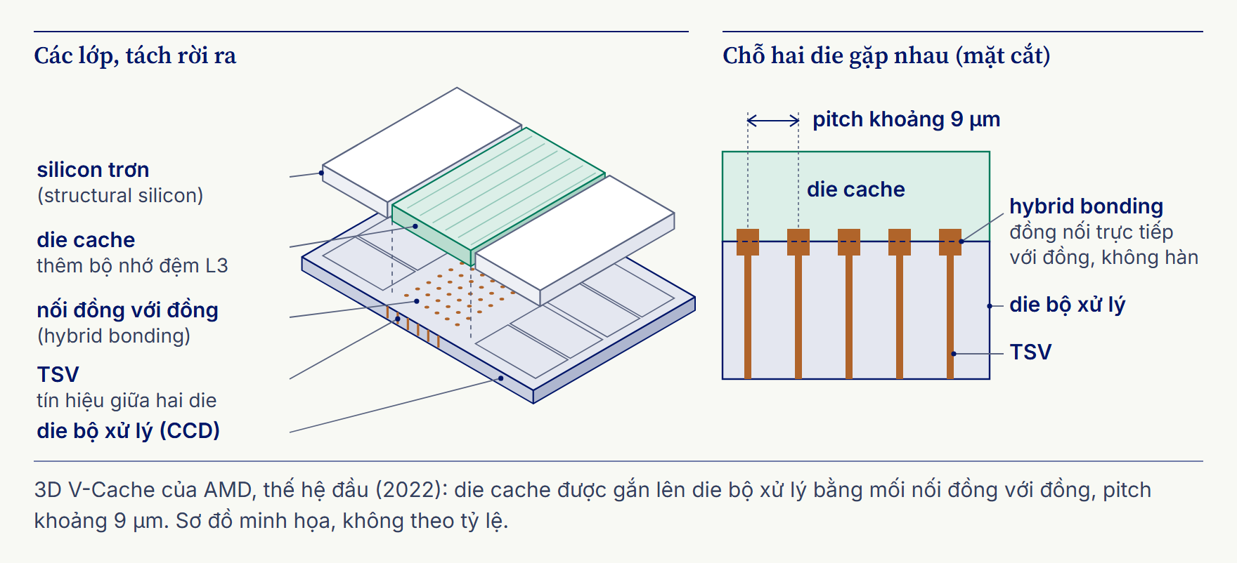
Microbump vẫn cách nhau vài chục micromet. Muốn đưa các kết nối lại gần nhau hơn nữa, người ta bỏ hẳn thiếc hàn. Với hybrid bonding, bề mặt đối diện của hai die được làm thật phẳng rồi áp vào nhau, và hai loại mối nối hình thành. Lớp điện môi, tức lớp cách điện mỏng bao quanh các điểm tiếp xúc (pad) bằng đồng, dính liền với lớp điện môi của die kia, còn mỗi pad đồng gắn thẳng vào pad đồng đối diện, tạo thành mối nối đồng với đồng (copper-to-copper bonding), không có thiếc hàn xen giữa. Hai loại mối nối ấy làm nên chữ “hybrid” trong tên gọi.7.9, 7.10
The method is already in products. Sony’s stacked image sensors have used it since 2016, the copper pads of the sensor chip bonded straight to those of the logic chip beneath it.7.11 Their first generation bonded at a pitch, the centre-to-centre distance between neighbouring connections, of 6 µm, and a Sony sensor examined in 2019 reached 3.1 µm.7.12 Between processor dies, hybrid bonding has been in products since 2022: AMD’s 3D V-Cache bonds an extra cache die, fast memory for the processor, onto the processor die on TSMC’s SoIC process, at a minimum pitch of 9 µm.7.9 Intel said in February 2024 that the first generation of its Foveros Direct will also use 9 µm, and the second will shrink the pitch to just 3 µm.7.13
Cách làm này đã có trong sản phẩm. Từ năm 2016, cảm biến ảnh xếp chồng của Sony đã dùng nó: các pad đồng của chip cảm biến được gắn thẳng vào pad đồng của chip logic bên dưới.7.11 Thế hệ đầu nối ở pitch (khoảng cách giữa tâm hai tiếp điểm kề nhau) 6 µm, và một cảm biến của Sony được phân tích năm 2019 đã xuống tới 3,1 µm.7.12 Giữa các die bộ xử lý, hybrid bonding có mặt trong sản phẩm từ năm 2022: 3D V-Cache của AMD gắn thêm một die cache, tức bộ nhớ tốc độ cao phục vụ bộ xử lý, lên die bộ xử lý. Việc ghép này dùng quy trình SoIC của TSMC, với pitch nhỏ nhất 9 µm.7.9 Tháng 2/2024, Intel cho biết Foveros Direct thế hệ đầu của hãng cũng sẽ nối ở pitch 9 µm, còn thế hệ thứ hai sẽ thu nhỏ pitch xuống chỉ còn 3 µm.7.13
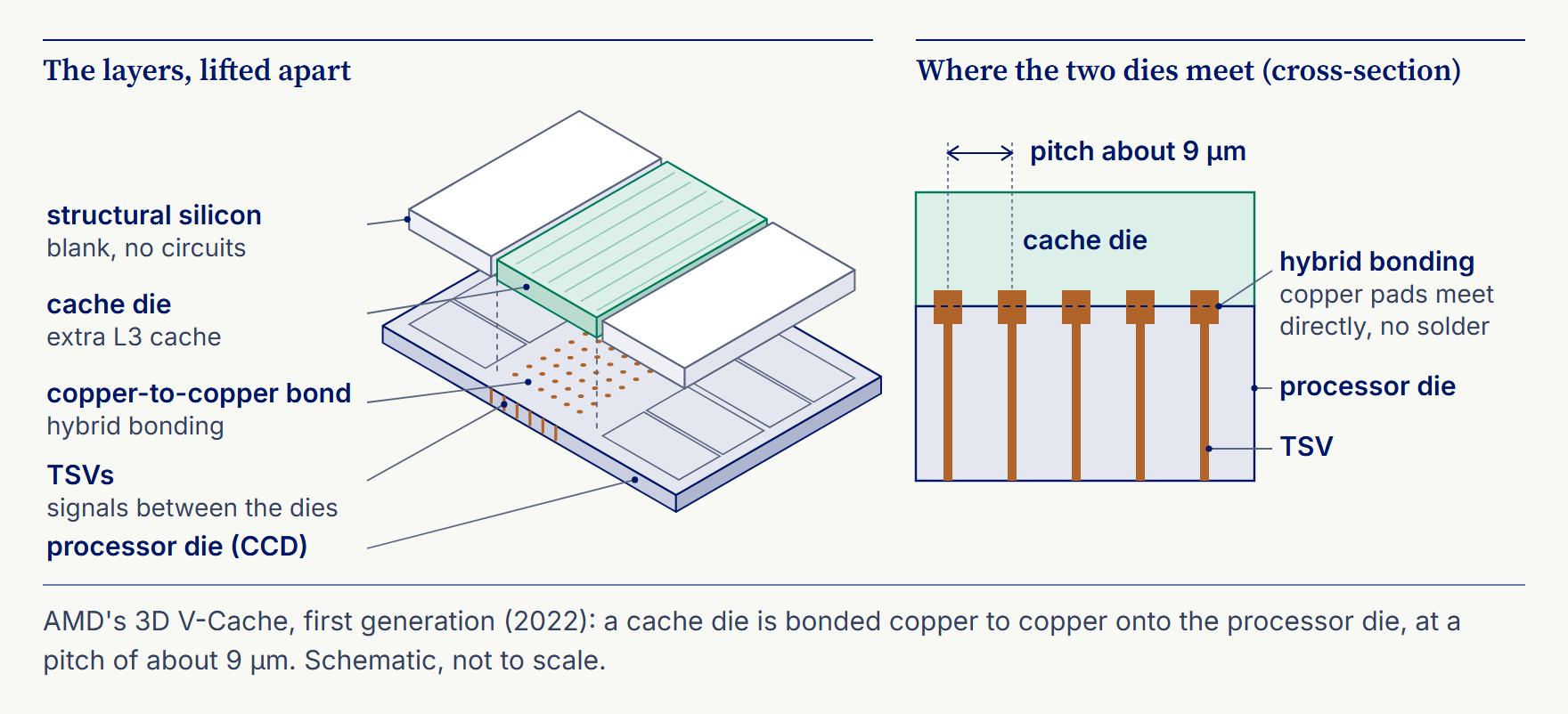
How the two dies meet matters as well. The upper die is usually turned face down, as in chapter 4’s flip chip, which joins a die to its package across its whole face. It can then meet the die below face to face, circuit side against circuit side, the shortest way between the two. Intel’s Foveros 2.5D works this way: an active die is bonded face to face onto a passive base die, which carries only wiring and is also known as a silicon interposer, so Intel counts the package as 2.5D, not 3D.7.14 Or the upper die’s face can land on the back of the die below, and signals then pass through that die by TSVs, as they climb a memory tower.
Cách hai die gặp nhau cũng quan trọng. Die bên trên thường được lật úp, như trong flip chip ở chương 4, cách gắn die vào package (phần đóng gói của chip) bằng các kết nối trải khắp bề mặt. Khi đó, die trên có thể ghép với die dưới mặt đối mặt (face-to-face bonding), mặt mạch áp vào mặt mạch, cho quãng đường ngắn nhất giữa hai die. Foveros 2.5D của Intel làm theo cách này: một die chứa mạch được ghép mặt đối mặt lên một die nền thụ động. Die nền chỉ mang dây dẫn, còn được gọi là silicon interposer, nên Intel xếp package này vào loại 2.5D chứ không phải 3D.7.14 Hoặc mặt die trên có thể đặt lên lưng die dưới, khi đó tín hiệu đi xuyên qua die dưới bằng TSV, giống như cách tín hiệu leo lên một tháp HBM.
Dies can be bonded one at a time onto a wafer, or a whole wafer onto another, wafer to wafer. TSMC’s SoIC offers both, at a bond pitch that starts below 10 µm,7.15 and joins the dies by hybrid bonding.7.9
Có thể gắn từng die một lên một wafer, hoặc gắn nguyên một wafer lên một wafer khác, tức wafer-to-wafer. SoIC của TSMC làm được cả hai cách, với pitch mối nối bắt đầu từ dưới 10 µm,7.15 và nối các die bằng hybrid bonding.7.9
How many more connections fit in the same square at each step
Ở mỗi nấc thang, cùng một ô vuông chứa thêm bao nhiêu kết nối
Every step in the history of packaging has fit more connections into the same area: first by spreading them across the package’s underside, then by bringing them closer together. A QFP carries its leads round its edge, 0.5 mm apart; a BGA spreads solder balls across its underside, about 1.0 mm apart; flip-chip bumps reach about 100 µm, microbumps a few tens of micrometres, and hybrid bonds between processor dies 9 µm in products since 2022, with about 6 µm reported for TSMC today and 3 µm announced by Intel.7.16, 7.13 The first two join a package to its printed circuit board (PCB); the rest join a die to its package or to another die. Spread across an area, the count grows with the square of the shrink: halve the pitch and four times as many connections fit.
Mỗi bước trong lịch sử đóng gói chip đều đưa thêm kết nối vào cùng một diện tích: trước hết bằng cách trải chúng khắp mặt dưới package, sau đó bằng cách đưa chúng xích lại gần nhau hơn. Chân của kiểu đóng gói QFP (Quad Flat Package) nằm quanh mép, cách nhau 0,5 mm; kiểu đóng gói BGA (ball grid array) trải bi hàn khắp mặt dưới, cách nhau chừng 1,0 mm; bump flip chip xuống tới khoảng 100 µm, microbump vài chục micromet, còn hybrid bonding giữa các die bộ xử lý đạt 9 µm trong sản phẩm từ năm 2022; nay TSMC được cho là đạt khoảng 6 µm, và Intel đã công bố mức 3 µm.7.16, 7.13 Hai loại đầu nối package với bo mạch in (PCB); các loại còn lại nối die với package hoặc với một die khác. Khi kết nối trải khắp một diện tích, số lượng tăng theo bình phương: giảm pitch đi một nửa thì đặt được gấp bốn lần.
The 10 × 10 mm squareÔ vuông 10 × 10 mm
Window 0.4 × 0.4 mmVùng phóng to 0,4 × 0,4 mm
Window 36 × 36 µmVùng phóng to 36 × 36 µm
the connection on the sliderloại kết nối đang chọnthe one you compare withloại đem ra so sánha coarser step, for scalemột nấc thô hơn, làm mốc so kích thướcthe window the next panel zooms intovùng được phóng to ở khung kế tiếp
- ConnectionLoại kết nối
- Microbumps, 40 µm (typical value)Microbump, 40 µm (giá trị điển hình)
- JoinsNối giữa
- a die to another die, or to an interposerdie với die, hoặc die với interposer
- In the 10 × 10 mm squareTrong ô vuông 10 × 10 mm
- 62,50062.500
- Per mm²Trên mỗi mm²
- 625625
- ComparedSo sánh
- Microbumps (40 µm): 625 times as many as BGA balls (1.0 mm)Microbump (40 µm): nhiều gấp 625 lần bi hàn BGA (1,0 mm)
- ExampleVí dụ
- a typical value inside the published range: 25 µm (UCIe’s 2.5D class) to 55 µm (Intel’s first EMIB), with Foveros at 36 µm and EMIB at 45 µm (as of 2024)một giá trị điển hình trong khoảng đã công bố: từ 25 µm (lớp 2.5D của UCIe) đến 55 µm (EMIB đời đầu của Intel); Foveros ở 36 µm, EMIB ở 45 µm (tính đến năm 2024)7.31, 7.13, 7.14
Shown: microbumps compared with BGA balls. Turn on JavaScript to step through the connections; the table lists every one.Đang hiển thị: microbump so với bi hàn BGA. Bật JavaScript để chuyển qua từng loại kết nối; bảng dưới đây liệt kê đủ các loại.
Every connection, counted in the 10 × 10 mm squareMọi loại kết nối, đếm trong ô vuông 10 × 10 mm
| ConnectionLoại kết nối | PitchPitch | In the squareTrong ô vuông | Per mm²Trên mỗi mm² | ExampleVí dụ |
|---|---|---|---|---|
| QFP leadsChân QFPedge ring, 4 × (10/p)vòng quanh cạnh, 4 × (10/p) | 0.5 mm0,5 mm | 8080 | 0.80,8 | a 10 × 10 mm LQFP at 0.5 mm (NXP SOT1699-1, JEDEC MS-026); the real part carries 64 leads, its corners empty (2016)một LQFP 10 × 10 mm, pitch 0,5 mm (NXP SOT1699-1, chuẩn JEDEC MS-026); linh kiện thật có 64 chân, bốn góc để trống (2016)7.26 |
| BGA ballsBi hàn BGAfull grid, (10/p)²lưới kín, (10/p)² | 1.0 mm1,0 mm | 100100 | 11 | Amkor’s ball grid arrays, offered at ball pitches from 0.4 mm to 1.0 mm, a common pitch (2020)các BGA của Amkor, có pitch bi hàn từ 0,4 mm đến 1,0 mm, trong đó 1,0 mm là pitch phổ biến (2020)7.28, 7.29 |
| Flip-chip bumpsBump flip chipfull grid, (10/p)²lưới kín, (10/p)² | 100 µm100 µm | 10,00010.000 | 100100 | standard-package bump pitches “at 100um and higher” (UCIe Consortium); Amkor’s flip-chip BGA reaches 90 µm (2023)pitch bump của package tiêu chuẩn từ 100 µm trở lên (UCIe Consortium); FCBGA của Amkor xuống tới 90 µm (2023)7.30, 7.28 |
| MicrobumpsMicrobumpfull grid, (10/p)²lưới kín, (10/p)² | 40 µm40 µm | 62,50062.500 | 625625 | a typical value inside the published range: 25 µm (UCIe’s 2.5D class) to 55 µm (Intel’s first EMIB), with Foveros at 36 µm and EMIB at 45 µm (as of 2024)một giá trị điển hình trong khoảng đã công bố: từ 25 µm (lớp 2.5D của UCIe) đến 55 µm (EMIB đời đầu của Intel); Foveros ở 36 µm, EMIB ở 45 µm (tính đến năm 2024)7.31, 7.13, 7.14 |
| Hybrid bonds in processors, in productionHybrid bonding trong bộ xử lý, đang sản xuấtfull grid, (10/p)²lưới kín, (10/p)² | 9 µm9 µm | about 1.23 millionkhoảng 1,23 triệu | about 12,300khoảng 12.300 | AMD’s 3D V-Cache, bonded on TSMC’s SoIC process; Intel describes its first-generation Foveros Direct at the same 9 µm (2022)3D V-Cache của AMD, nối bằng quy trình SoIC của TSMC; Intel mô tả Foveros Direct thế hệ đầu cũng ở pitch 9 µm (2022)7.9, 7.13 |
| Hybrid bonds in processors, announced by IntelHybrid bonding trong bộ xử lý, Intel mới công bốfull grid, (10/p)²lưới kín, (10/p)² | 3 µm3 µm | about 11.1 millionkhoảng 11,1 triệu | about 111,000khoảng 111.000 | Intel said in February 2024 that the second generation of Foveros Direct will shrink the pitch to 3 µm, giving no date; in image sensors, a Sony sensor already bonded at 3.1 µm (2019)tháng 2/2024, Intel cho biết thế hệ Foveros Direct thứ hai sẽ thu nhỏ pitch xuống còn 3 µm, chưa nêu thời điểm; với cảm biến ảnh, một cảm biến của Sony đã nối ở pitch 3,1 µm (2019)7.13, 7.12 |
Off the scale, the DIP. Its pins sit 2.54 mm apart in two rows outside the footprint, so a 10 mm body carries four per side, eight in all.7.27DIP nằm ngoài thang đo. Chân của nó cách nhau 2,54 mm, xếp thành hai hàng bên ngoài phần thân, nên thân dài 10 mm mang bốn chân mỗi bên, tổng cộng tám chân.7.27
Same pitch, different layout. At the QFP’s 0.5 mm pitch a full grid holds 400 connections, five times the edge’s 80, because an edge ring gives 4 × (10/p) positions and a grid (10/p)², a ratio of 10/(4p). That is the layout lesson. The QFP-to-BGA pair is the history lesson: packages moved to a coarser 1.0 mm pitch and still gained count.Cùng pitch, khác cách bố trí. Ở pitch 0,5 mm của QFP, một lưới kín chứa được 400 kết nối, gấp năm lần 80 vị trí quanh cạnh, vì một vòng quanh cạnh cho 4 × (10/p) vị trí còn một lưới cho (10/p)², tỷ số là 10/(4p). Đó là điều rút ra về cách bố trí. Cặp QFP và BGA cho thấy diễn biến lịch sử: package chuyển sang pitch thô hơn, 1,0 mm, mà số kết nối vẫn tăng.
Makers’ bases differ. Makers compare hybrid bonding with their own microbumps, not with this plate’s 40 µm. Intel says hybrid bonding gives “up to 10x finer interconnect density” than conventional microbumps (Foveros Direct brief, November 2025)7.10, and AMD says about 15× the density of 3D stacking with solder bumps (3D V-Cache product brief)7.32. This plate’s figure for 9 µm against 40 µm, about 19.75 times, is the geometric ratio for full grids.Mỗi hãng so với một mốc khác. Các hãng so hybrid bonding với chính microbump của họ, không phải với mốc 40 µm của hình này. Intel cho biết hybrid bonding cho mật độ liên kết điện dày hơn tới 10 lần so với microbump thông thường (tài liệu Foveros Direct, tháng 11/2025)7.10, còn AMD cho biết mật độ liên kết điện gấp khoảng 15 lần so với cách xếp chồng 3D dùng bump thiếc hàn (tài liệu giới thiệu 3D V-Cache)7.32. Con số của hình này cho 9 µm so với 40 µm, khoảng 19,75 lần, là tỷ số hình học cho các lưới kín.
Quick questionThử đoán xem
Compared with the connections between a package and its circuit board, about how many times more connections fit in the same area between chips stacked on microbumps?So với các kết nối giữa package và bo mạch in, giữa các chip xếp chồng nối bằng microbump, cùng một diện tích chứa được nhiều kết nối hơn khoảng bao nhiêu lần?
Show the answerXem đáp án
100 to 1,000 times: two to three orders of magnitude. The ladder above shows the geometry: a board’s balls at a 1.0 mm pitch against microbumps at 40 µm put 625 times as many connections in the same square, the ideal for a full grid. Hybrid bonds go further: at 9 µm, the same square holds about 12,300 times as many as the board’s balls. Makers give their own figures, each against its own base. Synopsys says that bonding stacked dies into one package, instead of several packages on a board, raises I/O density, the density of a chip’s input and output connections, about 100 times.7.17 AMD says its hybrid-bonded 3D V-Cache has over 200 times the interconnect density of a 2D chiplet on the same package, and over 15 times that of 3D stacking with microbumps.7.18 Intel says Foveros Direct has up to 10 times the interconnect density of conventional microbumps.7.10 All of these count how closely connections pack, not how much shorter the path between two chips becomes.
100 đến 1.000 lần, tức hai đến ba bậc độ lớn. Thang kết nối ở trên cho thấy phần hình học: so bi hàn của bo mạch ở pitch 1,0 mm với microbump ở pitch 40 µm, cùng một ô vuông chứa được số kết nối gấp 625 lần, con số lý tưởng khi kết nối phủ kín thành lưới. Hybrid bonding còn đi xa hơn: ở pitch 9 µm, cùng ô vuông ấy chứa được số kết nối gấp khoảng 12.300 lần số bi hàn của bo mạch. Các hãng đưa ra con số của riêng mình, mỗi con số so với một mốc khác nhau. Synopsys cho biết ghép các die xếp chồng vào cùng một package, thay vì nhiều package trên một bo mạch, làm mật độ I/O, tức mật độ các kết nối vào và ra của chip, tăng khoảng 100 lần.7.17 AMD cho biết 3D V-Cache dùng hybrid bonding có mật độ liên kết điện gấp hơn 200 lần so với chiplet 2D đặt trên cùng package, và gấp hơn 15 lần so với cách xếp chồng 3D bằng microbump.7.18 Intel cho biết Foveros Direct có mật độ liên kết điện dày hơn tới 10 lần so với microbump thông thường.7.10 Tất cả các con số này đo độ dày đặc của kết nối, chứ không đo quãng đường giữa hai chip ngắn đi bao nhiêu.
Which company offers which stacking platform
Hãng nào cung cấp nền tảng xếp chồng die nào
Stacking dies is called 3D packaging, though Intel counts its Foveros 2.5D, an active die on a passive base die, as 2.5D. Three chipmakers that also make wafers offer stacking platforms, each under its own name.
Xếp chồng die được gọi là kiểu đóng gói 3D, dù Intel xếp Foveros 2.5D của hãng, một die chứa mạch đặt trên một die nền thụ động, vào loại 2.5D. Ba hãng chip vừa đóng gói vừa sản xuất wafer cung cấp các nền tảng xếp chồng die, mỗi hãng một tên gọi riêng.
| Platform | How the dies are joined | Pitch and status, as stated |
|---|---|---|
| TSMC SoIC | Hybrid bonding;7.9 chip on wafer or wafer on wafer7.15 | Bond pitch “starts from the sub-10µm rule”; 3 nm chip stacking in volume production in 2025.7.15 6 µm today and 4.5 µm by 2029, as reported (eeNews Europe, April 2026)7.16 |
| Intel Foveros 2.5D | Microbumps; an active die stacked face to face on a passive base die, a silicon interposer7.14 | A 36 µm microbump pitch7.14 |
| Intel Foveros Direct | Hybrid bonding, copper to copper, on an active base die7.19 | 9 µm in the first generation; 3 µm for the second, stated February 2024, no date given.7.13 Up to 10 times the interconnect density of conventional microbumps (November 2025)7.10 |
| Samsung X-Cube | TSVs through the logic die: a 7 nm test chip stacked SRAM on logic (announced August 2020)7.20 | Mass production of a bump-less, copper-to-copper version planned for 2026, as Samsung said at its 2022 foundry forum (as reported, 3DInCites, April 2023).7.21 Samsung’s foundry page now names its 3D packages Cube-T, stacked with TSVs and microbumps and ready for mass production, while Cube-H, joined by bump-less copper-to-copper hybrid bonding, is still under development (October 2026)7.22 |
| Nền tảng | Các die được nối thế nào | Pitch và tình trạng, theo công bố |
|---|---|---|
| SoIC của TSMC | Hybrid bonding;7.9 gắn chip lên wafer hoặc wafer lên wafer7.15 | Pitch mối nối bắt đầu từ dưới 10 µm; xếp chồng chip 3 nm vào sản xuất hàng loạt năm 2025.7.15 Hiện ở mức 6 µm, theo lộ trình là 4,5 µm vào năm 2029 (theo eeNews Europe, tháng 4/2026)7.16 |
| Foveros 2.5D của Intel | Microbump; một die chứa mạch xếp chồng mặt đối mặt trên một die nền thụ động, tức silicon interposer7.14 | Pitch microbump 36 µm7.14 |
| Foveros Direct của Intel | Hybrid bonding, đồng với đồng, trên một die nền chứa mạch7.19 | 9 µm ở thế hệ đầu; 3 µm cho thế hệ thứ hai, công bố tháng 2/2024, chưa nêu thời điểm.7.13 Mật độ liên kết điện gấp tới 10 lần microbump thông thường (tháng 11/2025)7.10 |
| X-Cube của Samsung | TSV xuyên qua die logic: chip thử nghiệm 7 nm xếp chồng SRAM lên die logic (công bố tháng 8/2020)7.20 | Tại Samsung Foundry Forum 2022, hãng lên kế hoạch sản xuất hàng loạt phiên bản nối đồng với đồng không cần bump vào năm 2026 (theo 3DInCites, tháng 4/2023).7.21 Trang foundry của Samsung nay gọi các package 3D của hãng là Cube-T, xếp chồng bằng TSV và microbump, đã sẵn sàng sản xuất hàng loạt, còn Cube-H, nối bằng hybrid bonding đồng với đồng không cần bump, vẫn đang được phát triển (tháng 10/2026)7.22 |
How is TSMC's SoIC different from Samsung's X-Cube?SoIC của TSMC khác X-Cube của Samsung ở điểm nào?
Both stack dies with TSVs running through the lower die; they differ in the joint between the two. SoIC joins the dies by hybrid bonding, with no bumps.7.15, 7.9 In August 2020 Samsung announced X-Cube, a 7 nm test chip stacking SRAM, fast on-chip memory, on a logic die with TSVs.7.20 Samsung’s foundry page today lists a version joined by microbumps, with a bump-less, copper-to-copper version under development.7.22 The table above gives the pitches and status.
Cả hai đều xếp chồng die, với TSV xuyên qua die bên dưới; chỗ khác nhau là mối nối giữa hai die. SoIC nối các die bằng hybrid bonding, không cần bump.7.15, 7.9 Tháng 8/2020, Samsung công bố X-Cube, một chip thử nghiệm 7 nm xếp chồng SRAM, loại bộ nhớ tốc độ cao nằm ngay trên chip, lên một die logic bằng TSV.7.20 Trang foundry của Samsung hiện liệt kê một phiên bản nối bằng microbump, còn phiên bản nối đồng với đồng không cần bump vẫn đang được phát triển.7.22 Pitch và tình trạng nằm ở bảng trên.
Why chips are still set side by side
Vì sao cách đặt chip cạnh nhau vẫn được dùng
If hybrid bonding packs connections so densely, why not stack everything? Four reasons keep 2.5D packaging, chips set side by side on an interposer or a silicon bridge, in wide use.
Nếu hybrid bonding cho kết nối dày đặc đến thế, sao không xếp chồng mọi thứ? Có bốn lý do khiến kiểu đóng gói 2.5D, tức đặt các chip cạnh nhau trên một interposer hay một cầu silicon (silicon bridge), vẫn được dùng rộng rãi.
- Heat. Every die in a stack gives off heat, and the heat of the lower dies has to pass up through the dies above, so thermal management, keeping the stack cool, limits how high dies can be stacked.
- Yield. A bonded stack cannot be taken apart and repaired, so one faulty die found after bonding scraps the whole stack. As with a big die in chapter 1, the more parts that must all work, the lower the share of good stacks, the yield.
- Design matching. Dies bonded at a fine pitch have to be designed for each other, pad for pad, and chips are far too varied for every pair to be made that way.
- Cost. Hybrid bonding costs more, and a product that does not need the density does not need to pay for it.
- Nhiệt. Mỗi die trong chồng đều tỏa nhiệt, và nhiệt của các die bên dưới phải đi xuyên qua các die bên trên, nên quản lý nhiệt, tức giữ cho cả chồng đủ mát, giới hạn số die có thể xếp chồng.
- Tỷ lệ thành phẩm. Chồng die đã nối thì không tháo ra sửa được, nên chỉ một die hỏng phát hiện sau khi nối cũng khiến cả chồng phải bỏ. Cũng như với một die lớn ở chương 1, càng nhiều phần cùng phải chạy tốt thì tỷ lệ thành phẩm (yield) của chồng càng thấp.
- Thiết kế khớp nhau. Các die nối với nhau ở pitch nhỏ phải được thiết kế dành riêng cho nhau, khớp từng pad một, trong khi chip quá đa dạng để cặp nào cũng làm được như vậy.
- Chi phí. Hybrid bonding đắt hơn, và sản phẩm không cần mật độ kết nối cao thì chẳng cần trả khoản tiền ấy.
Many packages therefore use both. A package that stacks logic dies and sets the stack beside other dies on an interposer or bridge is what some makers call 3.5D packaging. Broadcom announced its 3.5D XDSiP platform on 5 December 2024, which it describes as combining 3D silicon stacking with 2.5D packaging; it stacks dies face to face and holds up to 12 HBM stacks and more than 6,000 mm² of silicon in one package.7.23 AMD’s Instinct MI300 series stacks up to eight compute dies on four I/O dies, which handle the connections to everything else, and links them to eight HBM stacks.7.24 NVIDIA’s Blackwell GPUs keep their two largest dies side by side instead, each about as large as a lithography machine can print in one go, joined by a chip-to-chip link carrying 10 terabytes of data per second, which makes them one GPU (NVIDIA, March 2024).7.25
Vì vậy, nhiều package ngày nay dùng cả hai. Package vừa xếp chồng các die logic vừa đặt chồng ấy cạnh những die khác trên interposer hay cầu silicon được một số hãng gọi là kiểu đóng gói 3.5D. Ngày 5/12/2024, Broadcom công bố nền tảng 3.5D XDSiP, theo mô tả của hãng là kết hợp xếp chồng silicon 3D với đóng gói 2.5D; nền tảng này xếp chồng các die mặt đối mặt và chứa tới 12 chồng HBM cùng hơn 6.000 mm² silicon trong một package.7.23 Dòng Instinct MI300 của AMD xếp tối đa tám die tính toán lên bốn I/O die, loại die phụ trách kết nối với mọi thứ còn lại, và nối chúng với tám chồng HBM.7.24 Ngược lại, GPU Blackwell của NVIDIA vẫn đặt cạnh nhau hai die lớn của nó, mỗi die gần bằng diện tích lớn nhất mà máy quang khắc in được trong một lần, nối với nhau bằng đường truyền giữa hai chip tải 10 terabyte dữ liệu mỗi giây để thành một GPU duy nhất (NVIDIA, tháng 3/2024).7.25
No rung of the ladder has replaced the others. One AI package can carry balls to the board, bumps to its interposer, microbumps inside its memory towers and copper bonds between its logic dies, each where it pays for itself.
Không nấc nào trên thang kết nối thay thế hẳn các nấc còn lại. Một package AI có thể cùng lúc mang bi hàn nối xuống bo mạch, bump nối với interposer, microbump trong các tháp bộ nhớ và mối nối đồng với đồng giữa các die logic, mỗi loại ở đúng chỗ xứng với chi phí của nó.