Chapter 6 of 10Chương 6/10 11 min11 phút
Side by side: chips on interposers and bridgesĐặt các chip cạnh nhau trên interposer và cầu silicon
Once, each die had a package of its own, and chips talked to each other through the circuit board they were soldered to. The largest AI accelerators cannot work that way. In each, the processor and its memory trade data so fast that the wiring between them matters as much as either chip, and even a package substrate they share is too coarse to carry it. So the dies are set side by side on a thin layer of much finer wiring, an interposer or a small silicon bridge, in a package the industry calls 2.5D.
Từng có thời mỗi die có một package (phần đóng gói của chip) riêng, và các chip trao đổi dữ liệu với nhau qua tấm bo mạch in (PCB) bên dưới. Những accelerator AI lớn nhất không thể làm như vậy. Ở mỗi accelerator, bộ xử lý và bộ nhớ của nó trao đổi dữ liệu nhanh đến mức đường dây nối giữa hai bên quan trọng chẳng kém chính hai con chip, và ngay cả một substrate (đế) dùng chung cũng quá thô để đáp ứng. Vì thế, người ta đặt các die cạnh nhau trên một lớp dây dẫn mịn hơn nhiều, là interposer hoặc những cầu silicon (silicon bridge) nhỏ, trong một kiểu package mà ngành gọi là 2.5D.
In this chapter
Trong chương này
- Why a package substrate falls short between the fastest chips
- Three ways to seat dies side by side: on silicon interposers, on RDL interposers and on silicon bridges
- Which companies offer which 2.5D platforms
- Why square panels are being tried in place of round wafers
- Vì sao substrate không theo kịp khi các chip trao đổi dữ liệu tốc độ cao
- Ba cách đặt die cạnh nhau: trên silicon interposer, trên RDL interposer và qua cầu silicon
- Những hãng nào đang cung cấp nền tảng 2.5D nào
- Vì sao panel vuông đang được thử thay cho wafer tròn
A substrate cannot keep up with how fast chips trade data
Substrate không theo kịp tốc độ trao đổi dữ liệu giữa các chip
In a flip-chip package, the subject of chapter 4, the die lies face down on bumps about 100 µm or more apart. The substrate under it, a small multilayer circuit board, carries its signals and power out to the solder balls that join it to the main board.6.1 That suits a single die. It stops suiting two dies that must work as one, such as a processor and the memory it reads from. How much data can cross between them depends largely on how many wires run from the edge of one die to the edge of the next, and that depends on how finely the wiring under them can be drawn.
Ở một package flip chip, chủ đề của chương 4, die nằm úp mặt xuống trên các bump cách nhau từ khoảng 100 µm trở lên. Substrate bên dưới, một tấm mạch nhỏ nhiều lớp, dẫn tín hiệu và điện năng của die ra các bi hàn nối package với bo mạch chính.6.1 Cách làm ấy hợp với một die đơn lẻ. Nó không còn hợp khi hai die phải làm việc như một, chẳng hạn một bộ xử lý và bộ nhớ cấp dữ liệu cho nó. Lượng dữ liệu đi qua được giữa hai die phần lớn tùy vào số đường dây chạy từ mép die này sang mép die kia, và con số ấy lại tùy vào việc lớp dây bên dưới có thể vẽ mịn đến mức nào.
This is where a substrate falls short. It is made the way circuit boards are, and its copper lines are wide and far apart next to the lines drawn on a silicon interposer or bridge, which can be a couple of micrometres wide or finer.6.2, 6.3 ASE puts a number on the gap: its silicon bridge carries nearly 200 times as many wires per millimetre of die edge, per wiring layer, as a traditional organic flip-chip package.6.4
Substrate hụt hơi chính ở chỗ này. Nó được chế tạo như một tấm bo mạch, nên các đường dây đồng của nó vừa to vừa thưa so với dây vẽ trên silicon interposer hay cầu silicon, có thể chỉ rộng chừng hai micromet, thậm chí mảnh hơn.6.2, 6.3 ASE đưa ra một con số cho khoảng cách ấy: trên mỗi milimet mép die, ở mỗi lớp dây, cầu silicon của hãng chứa được số đường dây nhiều gấp gần 200 lần so với package flip chip hữu cơ truyền thống.6.4
So a thin layer of much finer wiring goes under the dies, or under just their facing edges. The dies sit on it side by side, joined to it by microbumps: very small bumps, often copper pillars with a solder cap, usually about 25 to 55 µm apart, where standard flip-chip bumps sit about 100 µm or more apart. That distance, centre to centre, is the pitch, and chapter 7’s ladder shows how many more connections each step down fits into the same square.6.5, 6.6 The layer’s own wiring links the dies to each other. In an interposer, signals and power travelling between the board and the dies pass down through it to the substrate. The processor and its memory sit neither in separate packages nor one on top of the other, which is why the arrangement is called 2.5D: halfway between a flat package and a stack.
Vì vậy, người ta đặt dưới các die, hoặc chỉ dưới hai mép đối diện của chúng, một lớp mỏng có dây dẫn mịn hơn nhiều. Các die nằm cạnh nhau trên lớp ấy, nối với nó qua các microbump: những bump rất nhỏ, thường là trụ đồng có mũ thiếc hàn, cách nhau khoảng 25 đến 55 µm, trong khi bump flip chip tiêu chuẩn cách nhau từ khoảng 100 µm trở lên. Khoảng cách ấy, tính từ tâm bump này sang tâm bump kế bên, gọi là pitch; nấc thang ở chương 7 cho thấy mỗi lần pitch nhỏ đi, cùng một ô vuông chứa thêm được bao nhiêu kết nối.6.5, 6.6 Liên kết điện (interconnect) giữa các die chạy ngay trong lớp dây ấy. Với interposer, tín hiệu và điện năng đi giữa bo mạch và các die xuyên qua nó xuống substrate. Bộ xử lý và bộ nhớ của nó không nằm trong những package riêng, cũng không nằm chồng lên nhau, nên cách bố trí này mang tên 2.5D: ở lưng chừng giữa một package phẳng và một chồng die.
Packages built this way were on sale by 2011. That October Xilinx began shipping its Virtex-7 2000T, an FPGA (a chip whose logic can be rewired after it is made) built from four dies on one passive silicon interposer, which Xilinx called “the first application of 2.5-D IC stacking”.6.7 TSMC lists the chip among the 2012 products of its CoWoS process (chip on wafer on substrate), and says CoWoS has been in volume production since 2012.6.3
Đến năm 2011, kiểu package này đã có mặt trên thị trường. Tháng 10 năm ấy, Xilinx bắt đầu giao Virtex-7 2000T, một FPGA (loại chip có thể lập trình lại mạch logic sau khi sản xuất) gồm bốn die đặt trên cùng một silicon interposer thụ động. Xilinx gọi đây là “ứng dụng đầu tiên của kỹ thuật xếp chồng IC 2.5D”.6.7 TSMC xếp con chip này vào nhóm sản phẩm năm 2012 của quy trình CoWoS (chip on wafer on substrate) và cho biết CoWoS đã vào sản xuất hàng loạt từ năm 2012.6.3
Dies can sit side by side in three ways
Có ba cách để các die nằm cạnh nhau
A silicon interposer is a slab of silicon wider than all the dies on it, with fine wiring on top. TSVs, through-silicon vias, run down through it to carry signals and power between the substrate and the dies. Is it a small circuit board or a large chip? Closer to a chip: it is built on a silicon wafer, with copper wiring finer than any board’s, but it is usually passive, wiring with no transistors of its own.6.3, 6.7 Its weakness is size. It must be as large as all the dies together, and every signal and power via between the dies and the substrate has to pass through it.6.8 TSMC’s CoWoS-S takes an interposer of up to 3.3 times the reticle, the largest area a chipmaking scanner prints in one exposure, or about 2,700 mm²; for anything larger TSMC recommends CoWoS-L or CoWoS-R.6.3
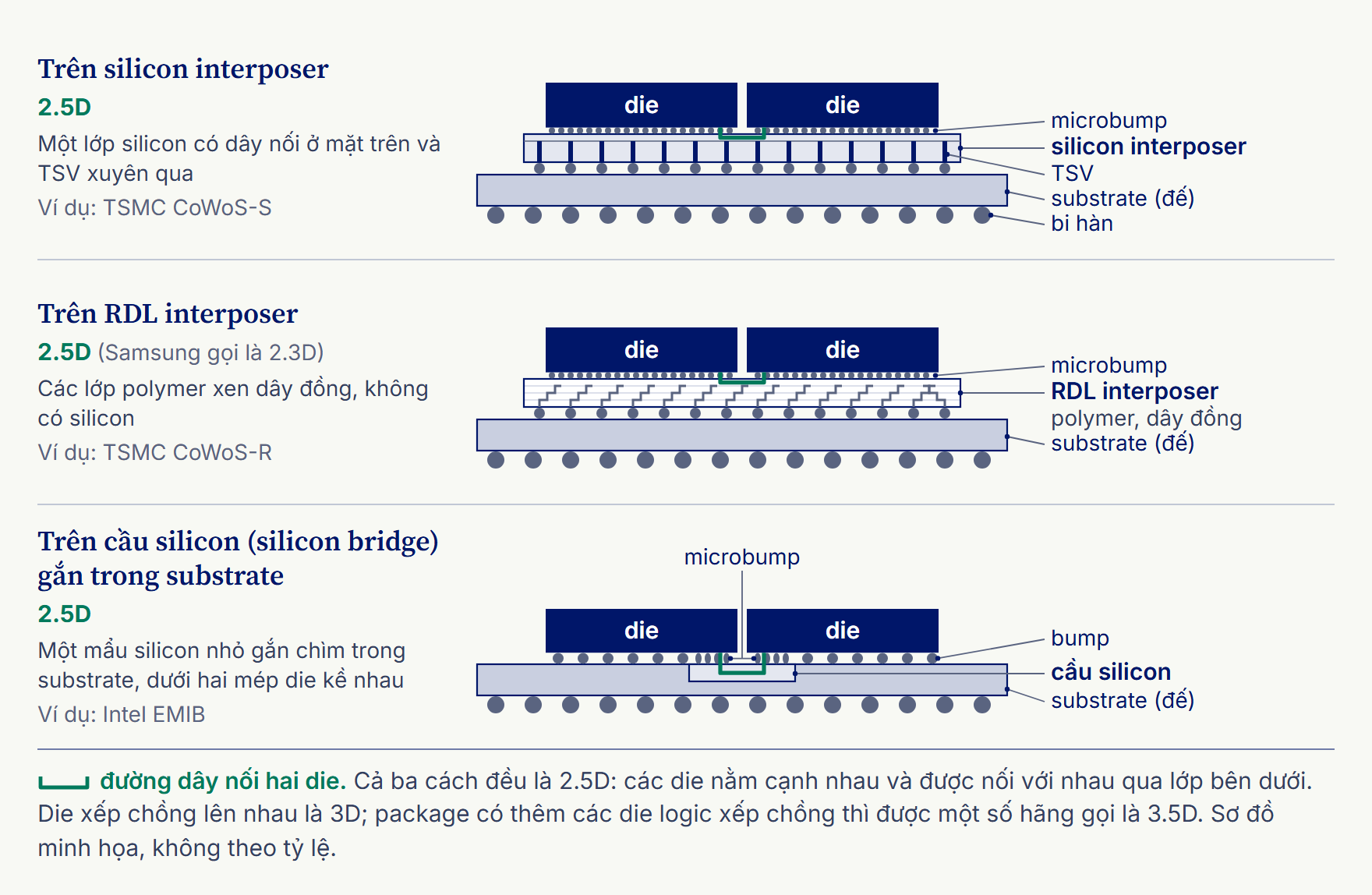
Silicon interposer là một tấm silicon rộng hơn tất cả các die đặt trên nó, mặt trên có dây dẫn mịn. Xuyên qua nó là các TSV (through-silicon via), những đường dẫn điện thẳng đứng đưa tín hiệu và điện năng qua lại giữa substrate và các die. Vậy nó giống một tấm mạch nhỏ hay một con chip lớn? Giống con chip hơn: người ta làm nó trên wafer silicon, dây đồng mịn hơn bất kỳ bo mạch nào, nhưng thường là thụ động, mang dây nối chứ không có bóng bán dẫn (transistor) nào.6.3, 6.7 Điểm yếu của nó là kích thước. Nó phải rộng bằng tất cả các die cộng lại, và mọi via tín hiệu, via cấp nguồn đi giữa các die và substrate đều phải xuyên qua nó.6.8 CoWoS-S của TSMC dùng được interposer rộng tới 3,3 lần reticle (vùng lớn nhất mà máy quang khắc in được trong một lần chiếu), tức khoảng 2.700 mm²; lớn hơn thế, TSMC khuyên dùng CoWoS-L hoặc CoWoS-R.6.3
An RDL interposer leaves the silicon out. It is built up from layers of polymer and copper wiring, the redistribution layers of chapter 4 spread wide enough to carry several dies, and is also called an organic interposer. Its wiring is far finer than a substrate’s, though not always as fine as silicon’s. The layers are also relatively flexible, which protects the joints of a large package from the strain of heating and cooling. Each time a package warms and cools, the chip and the substrate expand by different amounts; TSMC says the RDL layers buffer that mismatch and greatly reduce the strain on the bumps beneath.6.3 Samsung calls its own RDL-interposer packages 2.3D.6.9
RDL interposer thì bỏ hẳn silicon. Nó gồm nhiều lớp polymer xen dây đồng, tức các lớp RDL (redistribution layer) đã gặp ở chương 4, nay trải rộng đủ để đỡ nhiều die, nên còn có tên là organic interposer (interposer hữu cơ). Dây của nó mịn hơn dây trên substrate rất nhiều, dù không phải lúc nào cũng mịn bằng dây trên silicon. Các lớp này cũng tương đối mềm, nhờ vậy mối nối của một package lớn bớt chịu ứng suất mỗi khi nóng lên rồi nguội đi. Mỗi lần như thế, con chip và substrate giãn nở khác nhau; TSMC cho biết các lớp RDL làm đệm cho độ lệch ấy, giảm hẳn ứng suất dồn lên các bump bên dưới.6.3 Samsung gọi các package dùng RDL interposer của mình là 2.3D.6.9
A silicon bridge keeps silicon only where it is needed. A small piece of it, with several wiring layers, sits under the facing edges of two neighbouring dies and carries the dense links between them. The rest of each die connects through the ordinary package below.6.2, 6.8 Intel’s EMIB sets the bridge into the substrate itself. Only the bumps over the bridge need the fine microbump pitch, 45 µm in 2024, down from 55 µm; the rest of each die keeps a looser one.6.6, 6.8 Intel says HBM, the stacks of memory dies that sit beside AI processors (chapter 7), needs power delivered straight up from below with little noise. So it added TSVs through the bridge in EMIB-T.6.8 TSMC’s CoWoS-L and Samsung’s Cube-E set their bridges in an RDL interposer instead. TSMC calls its bridges LSI, local silicon interconnect.6.3, 6.9
Cầu silicon chỉ giữ silicon ở đúng chỗ cần đến. Một mẩu silicon nhỏ có vài lớp dây nằm dưới hai mép đối diện của hai die kề nhau và mang các liên kết điện dày đặc giữa chúng. Phần còn lại của mỗi die vẫn nối qua package thông thường bên dưới.6.2, 6.8 EMIB của Intel gắn chìm cầu ngay trong substrate. Chỉ những bump nằm trên cầu mới cần pitch microbump mịn, năm 2024 là 45 µm, giảm từ 55 µm; phần còn lại của mỗi die vẫn giữ pitch thưa hơn.6.6, 6.8 Theo Intel, bộ nhớ băng thông cao (high-bandwidth memory, HBM), tức những chồng die nhớ đặt cạnh bộ xử lý AI (chương 7), cần nguồn điện cấp thẳng từ bên dưới lên với rất ít nhiễu. Vì thế hãng bổ sung TSV xuyên qua cầu trong phiên bản EMIB-T.6.8 CoWoS-L của TSMC và Cube-E của Samsung thì gắn cầu silicon vào RDL interposer. TSMC gọi các cầu này là LSI (local silicon interconnect).6.3, 6.9
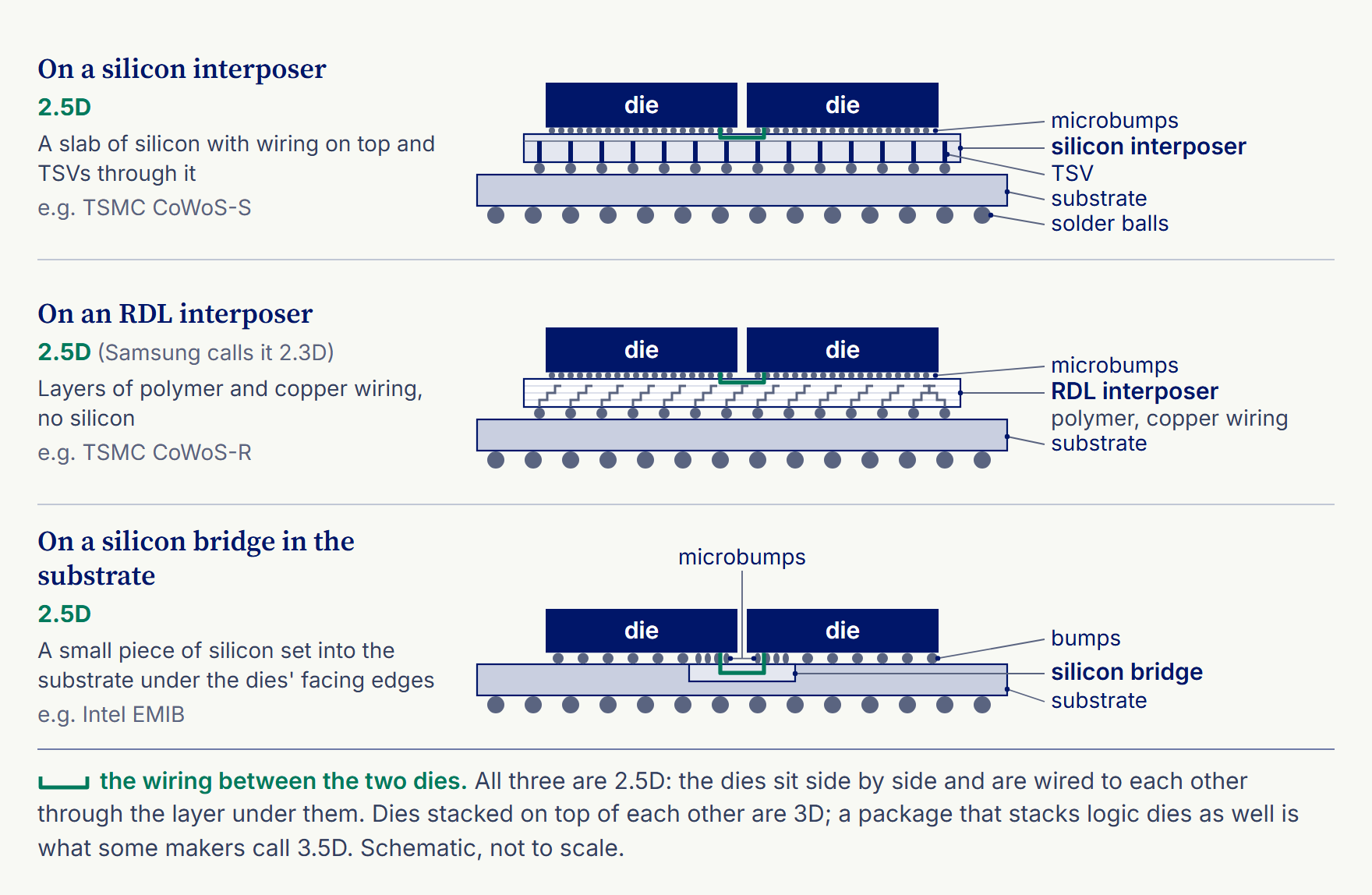
Dies can also be stacked on top of one another, joined by TSVs and microbumps or by copper bonded straight to copper. That is 3D, and a package that stacks logic dies and also sets dies side by side is what some makers call 3.5D; chapter 7 climbs that rung.
Die còn có thể xếp chồng lên nhau, nối bằng TSV và microbump, hoặc bằng đồng nối thẳng với đồng. Đó là 3D; còn package vừa xếp chồng các die logic vừa đặt die cạnh nhau thì được một số hãng gọi là 3.5D; chương 7 sẽ leo lên nấc thang ấy.
Who offers which 2.5D platform
Hãng nào cung cấp nền tảng 2.5D nào
Three chipmakers that also run their own wafer fabs, TSMC, Intel and Samsung, sell 2.5D packaging under their own names. So do OSATs, companies that package and test other firms’ chips: ASE, SPIL, which belongs to the same group, and Amkor. UMC, which makes chips for other companies, also makes silicon interposers for their packages. TSMC and Samsung each offer all three ways of seating dies side by side; the OSATs mostly offer fan-out layers, with or without a bridge.
Ba hãng chip có nhà máy sản xuất chip (fab) riêng là TSMC, Intel và Samsung đều bán dịch vụ đóng gói 2.5D dưới tên của mình. Các OSAT (công ty nhận đóng gói và kiểm thử chip cho hãng khác) cũng vậy: ASE, SPIL thuộc cùng tập đoàn với ASE, và Amkor. UMC, hãng nhận sản xuất chip cho các công ty khác, cũng làm silicon interposer cho package của họ. TSMC và Samsung đều có đủ cả ba cách đặt die cạnh nhau; các OSAT phần lớn làm lớp dây fan-out, có hoặc không kèm cầu silicon.
| Maker and platform | What the dies sit on | Status, as stated |
|---|---|---|
| TSMC CoWoS-S | A silicon interposer of up to about 2,700 mm², 3.3 times the reticle | In volume production since 20126.3 |
| TSMC CoWoS-R | An RDL interposer of polymer and copper, with lines 2 µm wide | In volume production since 20236.3 |
| TSMC CoWoS-L | An RDL interposer with small silicon bridges (LSI) set in it | In volume production since 2024;6.3 used for NVIDIA’s Blackwell B200, as reported (TechInsights)6.10 |
| TSMC InFO_oS and InFO_LSI | Fan-out wiring layers (chapter 5) on a substrate; InFO_LSI adds silicon bridges | InFO_LSI introduced in 20206.2 |
| Intel EMIB and EMIB-T | A silicon bridge set into the substrate; EMIB-T adds TSVs through the bridge for power | EMIB in high-volume manufacturing since 20176.8 |
| Samsung Cube-S, Cube-E and Cube-R | Cube-S: a silicon interposer. Cube-E: silicon bridges in an RDL interposer. Cube-R: an organic RDL interposer | Names on Samsung’s foundry page in 2026; its earlier 2.5D brand was I-Cube6.9, 6.11 |
| ASE FOCoS and FOCoS-Bridge | Fan-out wiring layers on a substrate; FOCoS-Bridge adds a silicon bridge | Part of ASE’s VIPack platform, introduced in June 20226.12 |
| SPIL | TSMC’s CoWoS-S, starting with the chip-on-wafer step | Taking its first such orders from TSMC, as reported (TrendForce, August 2024)6.13 |
| Amkor S-SWIFT | Fan-out wiring layers on a substrate, no interposer; Amkor calls it “a cost-effective alternative to traditional 2.5D TSV technology” | On offer (Amkor’s page, 2024)6.14 |
| UMC | Silicon interposer wafers for other companies’ 2.5D packages, finished by OSATs | “Ready for volume production” (UMC, undated)6.15 |
| Hãng và nền tảng | Die đặt trên gì | Tình trạng, theo công bố |
|---|---|---|
| TSMC CoWoS-S | Silicon interposer rộng tới khoảng 2.700 mm², gấp 3,3 lần reticle | Sản xuất hàng loạt từ năm 20126.3 |
| TSMC CoWoS-R | RDL interposer làm từ polymer và dây đồng, dây rộng 2 µm | Sản xuất hàng loạt từ năm 20236.3 |
| TSMC CoWoS-L | RDL interposer có gắn các cầu silicon nhỏ (LSI) | Sản xuất hàng loạt từ năm 2024;6.3 được dùng cho GPU Blackwell B200 của NVIDIA, theo TechInsights6.10 |
| TSMC InFO_oS và InFO_LSI | Các lớp dây fan-out (chương 5) trên substrate; InFO_LSI có thêm cầu silicon | InFO_LSI ra mắt năm 20206.2 |
| Intel EMIB và EMIB-T | Cầu silicon gắn chìm trong substrate; EMIB-T có thêm TSV xuyên qua cầu để cấp nguồn | EMIB sản xuất hàng loạt từ năm 20176.8 |
| Samsung Cube-S, Cube-E và Cube-R | Cube-S: silicon interposer. Cube-E: cầu silicon gắn trong RDL interposer. Cube-R: organic RDL interposer | Tên gọi trên trang foundry của Samsung năm 2026; trước đó Samsung bán các package 2.5D dưới tên I-Cube6.9, 6.11 |
| ASE FOCoS và FOCoS-Bridge | Các lớp dây fan-out trên substrate; FOCoS-Bridge có thêm cầu silicon | Thuộc nền tảng VIPack của ASE, ra mắt tháng 6/20226.12 |
| SPIL | CoWoS-S của TSMC, bắt đầu từ công đoạn chip-on-wafer | Được cho là đang nhận những đơn hàng đầu tiên loại này từ TSMC (theo TrendForce, tháng 8/2024)6.13 |
| Amkor S-SWIFT | Các lớp dây fan-out trên substrate, không cần interposer; Amkor gọi đây là “lựa chọn tiết kiệm chi phí thay cho công nghệ 2.5D dùng TSV truyền thống” | Đang được chào bán (trang của Amkor, 2024)6.14 |
| UMC | Wafer silicon interposer cho package 2.5D của các hãng khác, phần còn lại do OSAT hoàn tất | “Sẵn sàng sản xuất hàng loạt” (UMC, không ghi ngày)6.15 |
Who leads this market, and how far CoWoS capacity has fallen short of demand, is the subject of chapter 9.
Ai dẫn đầu thị trường này, và năng lực CoWoS thiếu hụt so với nhu cầu đến mức nào, là chuyện của chương 9.
Why square panels are being tried in place of round wafers
Vì sao panel vuông đang được thử thay cho wafer tròn
Most of the interposers and fan-out layers above start on a round wafer, and 300 mm is already the largest wafer in volume production, so the wafer cannot simply grow.6.2 The larger AI packages become, the fewer fit on each wafer and the more of it is lost around the curved edge, the way square bánh chưng, Vietnam’s rice cakes, packed into a round pot always leave gaps.6.16 Panel-level packaging builds the same layers on large rectangular panels instead. For large advanced packages, an IEEE roadmap, in a draft revision of March 2026, estimates that about 58% of a wafer’s area is put to use, against 76% of a 310 × 310 mm panel and 94% of a 600 × 600 mm one.6.2
Phần lớn các interposer và lớp fan-out kể trên đều bắt đầu từ một wafer tròn, và 300 mm đã là cỡ wafer lớn nhất đang sản xuất hàng loạt, nên wafer không thể cứ thế to thêm.6.2 Package cho AI càng lớn thì mỗi wafer chứa được càng ít, và phần bị bỏ phí quanh mép cong càng nhiều, giống như xếp bánh chưng vuông vào nồi tròn thì kiểu gì cũng hở những khoảng lớn.6.16 Panel-level packaging (đóng gói trên tấm panel) làm các lớp ấy trên những tấm panel chữ nhật lớn thay cho wafer. Với các package tiên tiến cỡ lớn, một lộ trình công nghệ của IEEE (bản sửa đổi dự thảo, tháng 3/2026) ước tính wafer chỉ tận dụng được khoảng 58% diện tích, so với 76% trên tấm panel 310 × 310 mm và 94% trên tấm 600 × 600 mm.6.2
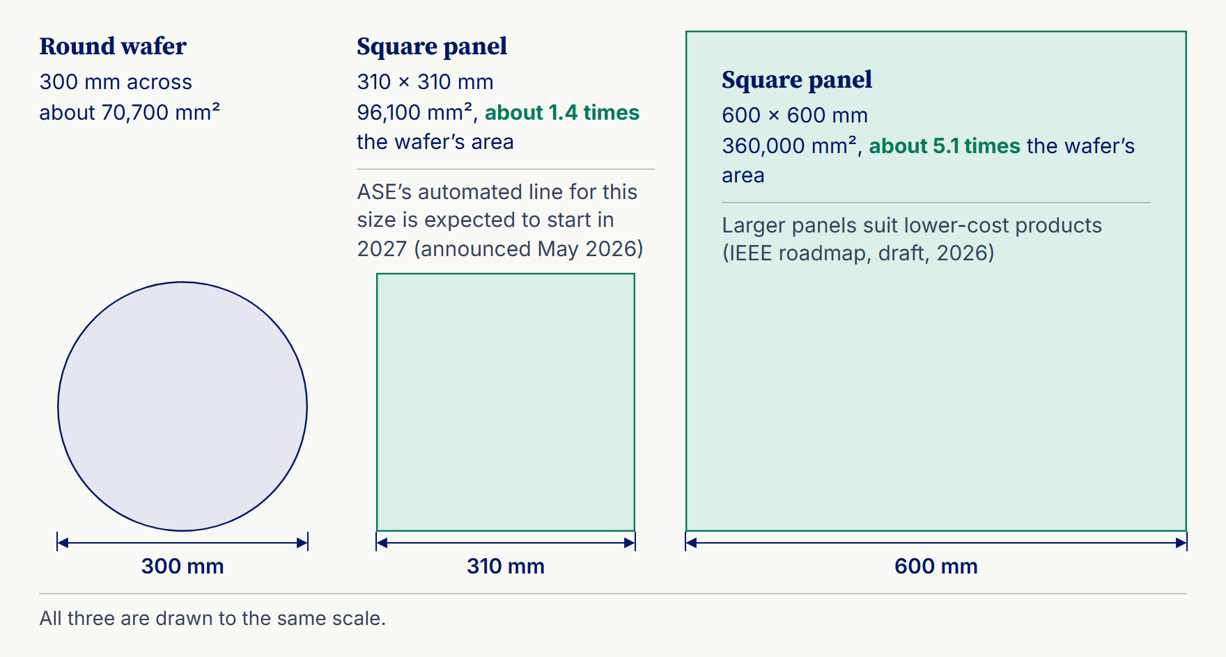
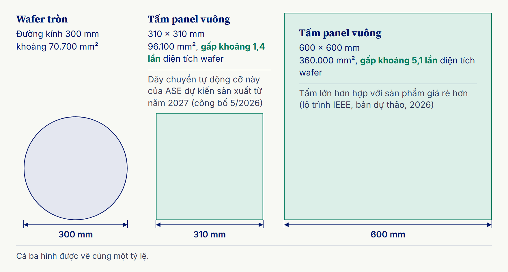
ASE announced in May 2026 an automated line for 310 × 310 mm panels, expected to enter production in the first half of 2027.6.16 TSMC has a pilot line for its own panel process, CoPoS (chip on panel on substrate), on 310 × 310 mm panels; volume production is expected in 2028 to 2029, as reported (TrendForce, June 2026).6.17 Samsung says the large interposer of its Cube-E is made on panels, and that of Cube-R on panels or wafers.6.9 The IEEE roadmap sees high-end makers settling on 310 mm panels while cheaper products favour larger ones.6.2
Tháng 5/2026, ASE công bố một dây chuyền tự động cho tấm panel 310 × 310 mm, dự kiến đi vào sản xuất trong nửa đầu năm 2027.6.16 TSMC có dây chuyền thử nghiệm cho quy trình panel của riêng mình, CoPoS (chip on panel on substrate), dùng tấm 310 × 310 mm. Hãng được cho là sẽ sản xuất hàng loạt trong khoảng năm 2028 đến 2029 (theo TrendForce, tháng 6/2026).6.17 Samsung cho biết interposer cỡ lớn của Cube-E được làm trên panel, còn của Cube-R thì trên panel hoặc wafer.6.9 Theo lộ trình của IEEE, các hãng ở phân khúc cao cấp đang dần thống nhất ở cỡ panel 310 mm, còn sản phẩm rẻ hơn thì chuộng tấm lớn hơn.6.2
Why use small silicon bridges instead of one big interposer?Vì sao dùng những cầu silicon nhỏ thay cho một tấm interposer lớn?
Mostly because of size. A full silicon interposer has to be as large as all the dies together, every signal and power via must pass through it, and beyond 3.3 times the reticle TSMC recommends CoWoS-L or CoWoS-R.6.3, 6.8 A bridge puts silicon only where neighbouring dies meet. Intel describes EMIB as “a very small bridge die with multiple routing layers, instead of the large silicon interposer”, needing fine microbumps “at the bridge only”, and calls a locally embedded bridge the more cost-effective option for links between logic dies and between logic and HBM.6.8 TSMC has moved the same way, saying its development focus has shifted from the original silicon interposer to interposers with multiple embedded bridges.6.18 A full interposer still gives fine wiring under the whole area, not only at the die edges, and it has the longest record in volume production, since 2012.6.3
Chủ yếu vì kích thước. Một silicon interposer nguyên tấm phải rộng bằng tất cả các die cộng lại, mọi via tín hiệu, via cấp nguồn đều phải xuyên qua nó, và với interposer vượt quá 3,3 lần reticle, TSMC khuyên dùng CoWoS-L hoặc CoWoS-R.6.3, 6.8 Cầu silicon chỉ đặt silicon ở nơi hai die kề nhau gặp nhau. Intel mô tả EMIB là “một die cầu rất nhỏ có nhiều lớp dây, thay cho tấm silicon interposer lớn”, chỉ cần microbump mịn “ở riêng phần cầu”, và coi cầu gắn cục bộ là lựa chọn tiết kiệm chi phí hơn cho liên kết điện giữa các die logic với nhau và giữa logic với HBM.6.8 TSMC cũng đi theo hướng ấy: hãng cho biết trọng tâm phát triển đã chuyển từ silicon interposer nguyên bản sang các interposer có nhiều cầu silicon gắn bên trong.6.18 Dù vậy, interposer nguyên tấm vẫn cho dây mịn trên toàn bộ diện tích chứ không riêng ở mép die, và có lịch sử sản xuất hàng loạt lâu nhất, từ năm 2012.6.3
What holds panel-level packaging back?Điều gì đang cản bước panel-level packaging?
Mostly what comes with a large, thin panel. An IEEE roadmap (a draft revision, March 2026) lists the problems. The panel warps, which upsets the focus and alignment of the patterns drawn on it. The dies set on it drift slightly out of place, more so the farther they sit from the centre. Each layer must line up with the last across a far larger area, and tools and steps made for round wafers, such as spin coating, do not carry over. Nor is there yet a standard panel size for the whole industry. For now, wiring on panels is coarser as well: the roadmap puts the lines and gaps most common in early panel production at about 8 to 15 µm.6.2
Chủ yếu là những khó khăn đi kèm một tấm panel lớn và mỏng. Lộ trình công nghệ của IEEE (bản sửa đổi dự thảo, tháng 3/2026) liệt kê các trở ngại. Tấm panel bị cong vênh, làm lệch tiêu điểm và độ khớp của các hình mẫu vẽ trên nó. Các die đặt lên panel bị xê dịch chút ít, càng xa tâm càng lệch nhiều. Mỗi lớp phải khớp với lớp trước trên một diện tích lớn hơn hẳn, và nhiều thiết bị, công đoạn làm cho wafer tròn, như phủ quay (spin coating), không đem sang dùng được. Ngành cũng chưa có một cỡ panel chuẩn chung cho mọi hãng. Hiện dây dẫn trên panel cũng thô hơn: theo lộ trình này, đường dây và khoảng cách giữa chúng phổ biến nhất trong giai đoạn đầu của sản xuất panel là khoảng 8 đến 15 µm.6.2