Chapter 5 of 10Chương 5/10 11 min11 phút
Packaging an RF filter without touching its surfaceĐóng gói chip lọc sóng mà không cần chạm vào bề mặt
A smartphone carries dozens of small filter chips, each with one job: to let one band of radio signals through and block the rest. Each makes an unusual demand of its package: nothing may touch the chip’s working surface. Following that package from a ceramic box to a dome built on the wafer, the thin disc the chips are made on, shows what packaging engineers weigh at every step. For these filters the wafer is a crystal such as lithium tantalate, not silicon.5.1 The dome is a wafer-level package, built before the wafer is cut, so the chapter starts there.
Một chiếc điện thoại thông minh mang trong mình vài chục con chip lọc sóng nhỏ, mỗi con chỉ làm một việc: cho một dải tín hiệu vô tuyến đi qua và chặn mọi dải còn lại. Loại chip này đặt ra cho package (phần đóng gói của chip) một yêu cầu khác thường: không gì được chạm vào bề mặt làm việc của nó. Package ấy đã đi từ chiếc hộp gốm đến mái vòm dựng ngay trên wafer, tức đĩa mỏng chứa các con chip, và mỗi bước trên chặng đường đó cho thấy kỹ sư đóng gói chip phải cân nhắc những gì. Với loại chip lọc sóng này, wafer là một tinh thể như lithium tantalate chứ không phải silicon.5.1 Mái vòm là một kiểu đóng gói ở cấp wafer (wafer-level packaging), làm trước khi cắt wafer, nên chương này bắt đầu từ đó.
In this chapter
Trong chương này
- What a wafer-level package is: fan-in, fan-out and TSMC’s InFO
- Why a phone’s RF filter needs air over its surface
- How the filter’s package shrank from a ceramic box
- How a dome is built over each filter on the wafer
- How materials are chosen and stress is simulated over the chip’s life
- How small the finished package is
- Đóng gói chip ở cấp wafer là gì, và fan-in, fan-out, InFO khác nhau ra sao
- Vì sao chip lọc sóng trong điện thoại cần khoảng trống phía trên bề mặt
- Package của chip lọc sóng đã thu nhỏ ra sao kể từ chiếc hộp gốm
- Mái vòm được dựng cho từng chip lọc sóng ngay trên wafer như thế nào
- Vật liệu được chọn và ứng suất được mô phỏng ra sao qua vòng đời con chip
- Package hoàn chỉnh nhỏ đến mức nào
How fan-in, fan-out and InFO package chips on the wafer
Fan-in, fan-out và InFO đóng gói chip ngay trên wafer ra sao
Chips are made by the hundred, or for small chips like these filters by the thousand, on a wafer, and most are cut apart into dies first and packaged one by one. Wafer-level packaging turns that round: the package’s wiring and solder balls are added to a whole wafer of dies at once, every die in the same steps, and the wafer is cut only at the end.5.2 What comes out needs no further package and can be soldered straight onto a board or into a module.
Một tấm wafer chứa được hàng trăm con chip, với chip nhỏ như chip lọc sóng thì hàng nghìn con; thông thường, người ta cắt wafer thành từng die rồi mới đóng gói từng con một. Đóng gói chip ở cấp wafer làm theo chiều ngược lại. Các lớp dây dẫn và bi hàn của package được làm cùng lúc cho mọi die trên cả tấm wafer, die nào cũng qua đúng những bước như nhau. Wafer chỉ bị cắt ra ở bước cuối.5.2 Thứ thu được không cần đóng gói thêm, có thể hàn thẳng lên bo mạch hoặc vào một module.
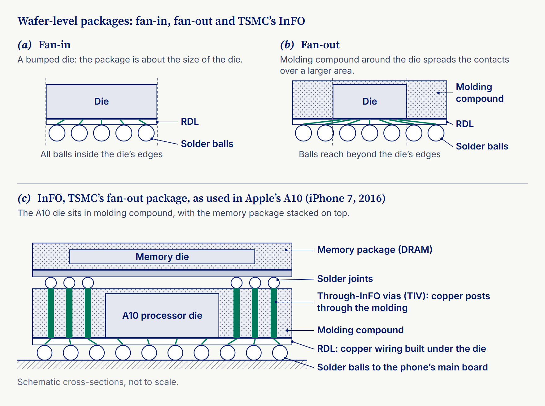
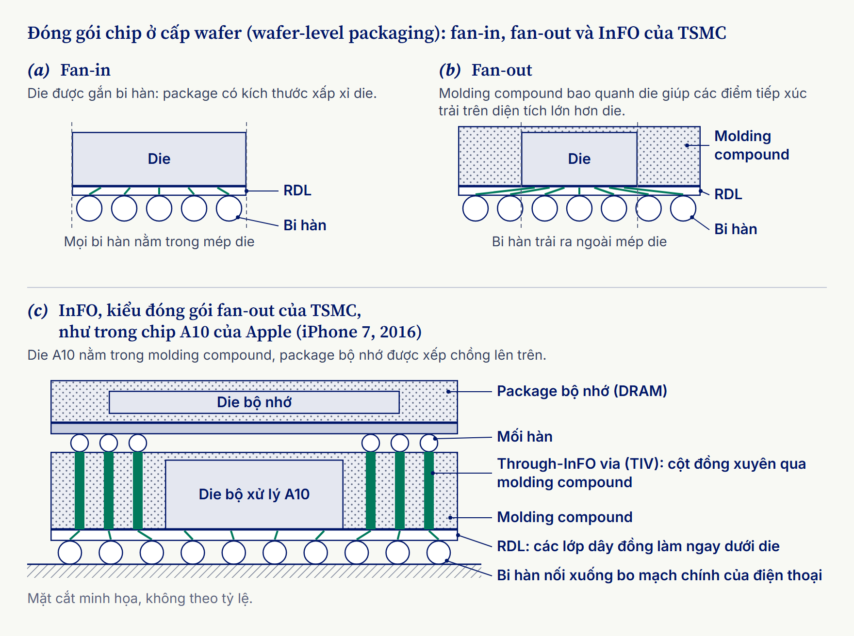
There are two kinds. In a fan-in package, often called a WLCSP (wafer-level chip-scale package), the wiring is built on the uncut wafer and stays inside each die’s own outline: the package is a bumped die, about the size of the die itself.5.2 That wiring is an RDL (redistribution layer), thin copper lines that move the die’s pads to where the solder balls go, as chapter 4’s flip chip does under its bumps. In a fan-out package the dies are cut apart first and placed, with room between them, in molding compound, the epoxy that seals most chip packages, to form a new, artificial wafer; the RDL is built over them and runs out past each die’s edges, so the contacts spread over an area larger than the die.5.2 A small die with many connections needs that extra room, because its balls no longer have to fit under the die.
Có hai kiểu. Ở kiểu fan-in, thường gọi là WLCSP (wafer-level chip-scale package), dây dẫn được làm ngay trên wafer chưa cắt và chỉ nằm gọn trong đường viền của từng die. Package khi ấy thực chất là một die đã gắn bi hàn, to xấp xỉ chính con die.5.2 Lớp dây dẫn ấy là RDL (redistribution layer), những đường đồng mảnh đưa các điểm tiếp xúc (pad) của die tới chỗ đặt bi hàn, giống như flip chip ở chương 4 làm với các bump của nó. Ở kiểu fan-out, các die được cắt rời trước, rồi đặt cách nhau trong lớp nhựa bọc (molding compound), loại nhựa epoxy bịt kín hầu hết các package, để tạo thành một wafer nhân tạo mới. RDL được làm phủ lên trên, trải ra quá mép từng die, sang cả phần nhựa xung quanh, nhờ vậy các điểm tiếp xúc dàn ra trên một diện tích lớn hơn die.5.2 Một die nhỏ mà cần nhiều kết nối sẽ cần khoảng rộng thêm ấy, vì bi hàn không còn phải chen hết bên dưới die.
TSMC’s fan-out package is called InFO, short for integrated fan-out. It shipped in Apple’s A10 processor, in the iPhone 7 of 2016, as a teardown of the phone confirmed.5.3 The phone’s memory, in a package of its own, sits stacked on top; TSMC has made InFO in volume since 2016.5.4 This phone version, InFO_PoP, has no substrate, the small multilayer board most packages are built on, and TSMC gives that as one reason its stack is thinner than one built on a substrate.5.4
Kiểu fan-out của TSMC mang tên InFO (Integrated Fan-Out). InFO có mặt trong bộ xử lý A10 của Apple, lắp trên chiếc iPhone 7 năm 2016, như kết quả mổ xẻ chiếc điện thoại này đã xác nhận.5.3 Bộ nhớ của máy nằm trong một package riêng, xếp chồng lên trên; TSMC đã sản xuất hàng loạt InFO từ năm 2016.5.4 Phiên bản dùng cho điện thoại này, InFO_PoP, không cần substrate (đế), tấm mạch nhỏ nhiều lớp làm nền cho hầu hết các package; theo TSMC, đó là một lý do khiến chồng package này mỏng hơn loại dựng trên substrate.5.4
The filter at the heart of this chapter is packaged at wafer level too, but its package faces a problem the A10’s does not: the chip’s surface must be left untouched.
Chip lọc sóng, nhân vật chính của chương này, cũng dùng kiểu đóng gói ở cấp wafer, nhưng package của nó vướng một bài toán mà A10 không gặp: bề mặt chip không được để bất cứ thứ gì chạm vào.
What an RF filter does, and why it needs air
Chip lọc sóng làm gì và vì sao cần khoảng trống phía trên bề mặt
A phone’s antenna picks up many signals at once. An RF filter lets through the radio-frequency (RF) band the phone needs and blocks the others, so the radio hears only its own band. Mobile phones once needed only a handful of filters. As phones took on more and more cellular bands, from 2G to 4G LTE, beside Wi-Fi, Bluetooth and satellite signals, the count climbed: by early 2016 a smartphone carried about 50 filters of all kinds, a Qualcomm figure as reported (Microwaves & RF, January 2016).5.5
Ăng-ten điện thoại thu cùng lúc rất nhiều tín hiệu. Chip lọc sóng cho dải tần RF (radio frequency) mà máy cần đi qua và chặn các dải còn lại, để bộ thu vô tuyến chỉ nhận đúng dải tần của mình. Điện thoại di động thời đầu chỉ cần vài chip lọc sóng. Khi điện thoại phải xử lý ngày càng nhiều dải tần di động, từ 2G đến 4G LTE, bên cạnh Wi-Fi, Bluetooth và tín hiệu vệ tinh, con số ấy tăng dần. Đến đầu năm 2016, một chiếc điện thoại thông minh đã mang khoảng 50 chip lọc sóng đủ loại, theo con số của Qualcomm mà Microwaves & RF đưa tin (tháng 1/2016).5.5
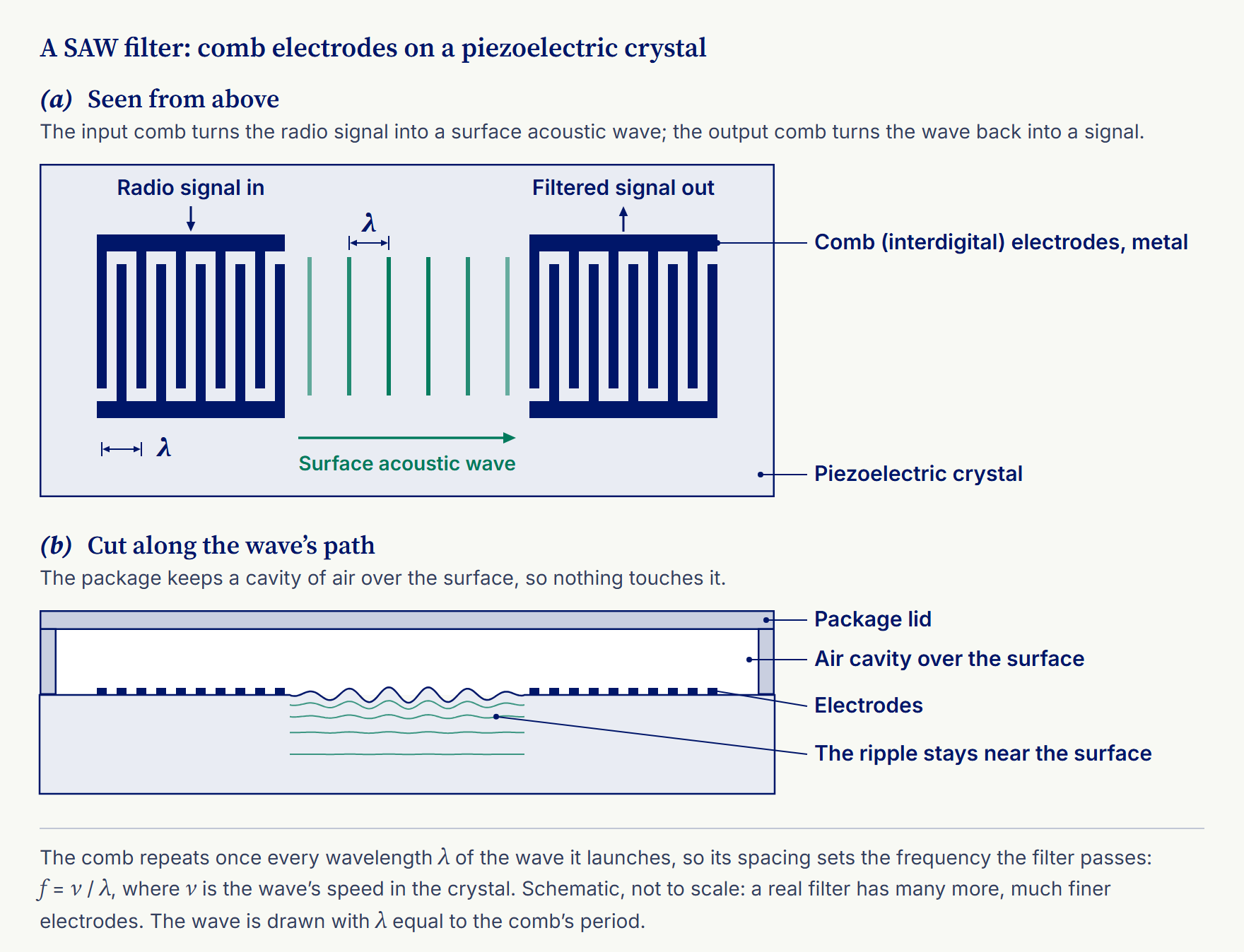
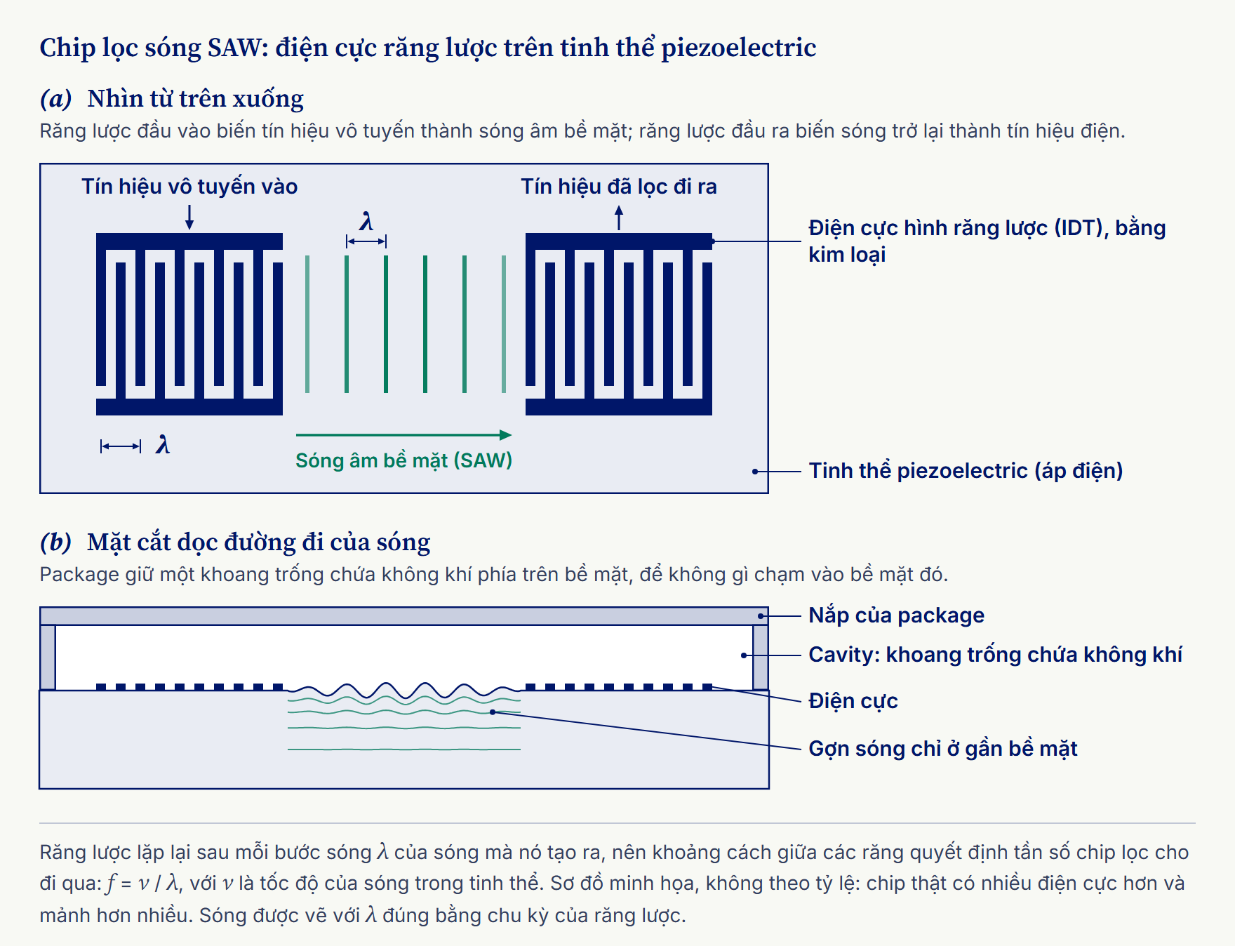
Phones use two common kinds, and this chapter follows the SAW (surface acoustic wave) filter. On a piezoelectric crystal, a material that changes shape when a voltage is applied, sit two sets of metal electrodes, one at the input and one at the output. Each set is shaped like two combs with their teeth interlocked: an interdigital transducer. The input comb turns the radio signal into a tiny ripple, a sound wave that runs along the crystal’s surface; the output comb turns the ripple back into a signal.5.6 Only a wave whose length matches the comb’s period, the distance from one finger to the next finger of the same comb, is launched strongly, so that period sets the frequency that passes. In the other kind, the BAW (bulk acoustic wave) filter, the wave bounces up and down through the thickness of a thin piezoelectric film, which must also be left free to vibrate.5.1
Điện thoại dùng hai loại chip lọc sóng phổ biến, và chương này theo chân chip lọc sóng SAW (surface acoustic wave), loại dùng sóng âm chạy trên bề mặt. Trên một tinh thể piezoelectric (áp điện), loại vật liệu đổi hình dạng khi có điện áp đặt vào, có hai bộ điện cực kim loại, một ở đầu vào, một ở đầu ra. Mỗi bộ trông như hai chiếc lược cài răng vào nhau, gọi là điện cực răng lược (interdigital transducer, IDT). Răng lược đầu vào biến tín hiệu vô tuyến thành một “gợn sóng” rất nhỏ, tức một sóng âm chạy dọc bề mặt tinh thể. Răng lược đầu ra biến gợn sóng ấy trở lại thành tín hiệu điện.5.6 Chỉ những sóng có bước sóng khớp với chu kỳ của răng lược, tức khoảng cách từ một răng tới răng kế tiếp của cùng một chiếc lược, mới được kích mạnh, nên chu kỳ ấy quyết định tần số nào đi qua được. Ở loại thứ hai, chip lọc sóng BAW (bulk acoustic wave), sóng dội lên xuống theo bề dày của một màng piezoelectric mỏng, và màng ấy cũng phải được để trống cho dao động.5.1
That ripple is what makes the filter hard to package. The wave lives on the surface, so anything resting on it, molding compound or glue, would damp it or distort it, and the filter would no longer do its job. Its package must keep a cavity, a pocket of air, over the working surface, while it still protects the chip and connects it to the phone’s circuit board or radio module like any other package.5.6, 5.1
Chính gợn sóng ấy khiến chip lọc sóng khó đóng gói. Sóng chạy trên bề mặt, nên bất cứ thứ gì đè lên đó, dù là lớp nhựa bọc hay keo, cũng sẽ làm sóng yếu đi hoặc méo đi, và chip lọc sóng không còn làm đúng việc của nó. Package vì thế phải chừa một khoang trống (cavity) chứa không khí phía trên bề mặt làm việc, trong khi vẫn bảo vệ con chip và nối nó với bo mạch in (PCB) hoặc module vô tuyến của điện thoại như mọi package khác.5.6, 5.1
The filter's package shrinks from a ceramic box
Package của chip lọc sóng thu nhỏ dần từ chiếc hộp gốm
The first answer was a box. Older SAW filters sat in a ceramic package, a small hollow ceramic body sealed with a metal lid; inside, the chip was joined to the package by wire bonding, chapter 3’s fine wires welded from pads at the die’s edge.5.7, 5.1 The air in the box kept the surface free, and the airtight, or hermetic, seal kept out moisture.
Lời giải đầu tiên là một chiếc hộp. Các chip lọc sóng SAW thế hệ trước nằm trong một package gốm (ceramic package), tức một thân gốm rỗng nhỏ đậy kín bằng nắp kim loại. Bên trong, con chip nối với package bằng nối dây (wire bonding), những sợi dây mảnh hàn từ các pad ở mép die mà chương 3 đã kể.5.7, 5.1 Khoảng không khí trong hộp giữ cho bề mặt chip thoáng, còn kiểu đóng gói kín ngăn hơi ẩm lọt vào.
One such package of 1996 measured 5.0 × 5.0 × 1.35 mm. Phones, meanwhile, needed more filters and grew thinner, so the package had to shrink. By 2020 a wafer-level filter package measured about 1.0 × 0.85 × 0.3 mm, roughly 130 times smaller by volume than in 1996, as a 2025 review of SAW packaging charts it.5.1
Một package như thế, năm 1996, có kích thước 5,0 × 5,0 × 1,35 mm. Trong khi đó, điện thoại cần ngày càng nhiều chip lọc sóng và ngày càng mỏng, nên package buộc phải thu nhỏ. Đến năm 2020, một package chip lọc sóng ở cấp wafer chỉ còn khoảng 1,0 × 0,85 × 0,3 mm, thể tích nhỏ hơn chừng 130 lần so với năm 1996, theo biểu đồ trong một bài tổng quan năm 2025 về đóng gói chip lọc sóng SAW.5.1
In 2019 Murata began volume production of SAW filters 0.9 × 0.7 mm in length and width, about 37% smaller in footprint than a conventional 1.1 × 0.9 mm filter; it gave no height.5.8 The same announcement counted the SAW devices alone in a phone: a mid-range phone sold in one region then used 14 or 15, and a premium model built to work worldwide as many as 30 to 40.5.8
Năm 2019, Murata bắt đầu sản xuất hàng loạt chip lọc sóng SAW có chiều dài và chiều rộng 0,9 × 0,7 mm, nhỏ hơn khoảng 37% về diện tích so với loại 1,1 × 0,9 mm thông thường; Murata không công bố độ dày.5.8 Cũng trong thông cáo ấy, hãng đếm riêng số linh kiện SAW trong một chiếc điện thoại: một điện thoại tầm trung bán ở một khu vực khi đó dùng 14 hoặc 15 con, còn một mẫu cao cấp dùng được ở khắp thế giới có thể cần tới 30 đến 40.5.8
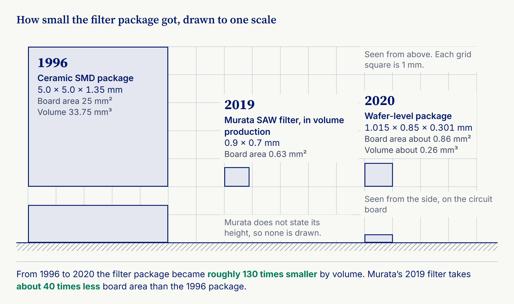
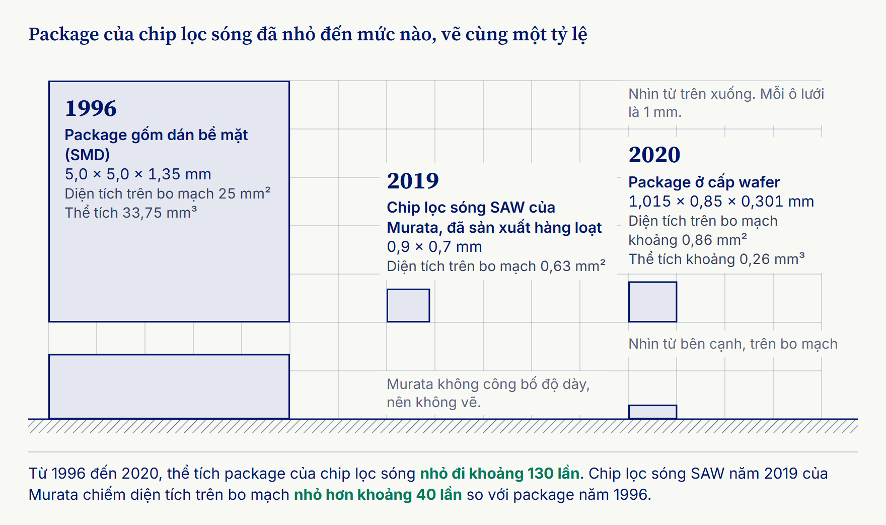
Along the way the ceramic box gave way to wafer-level packages, and bond wires gave way to flip chip soldering, the chip set face down on bumps.5.1
Trên chặng đường ấy, chiếc hộp gốm dần nhường chỗ cho các package ở cấp wafer, còn dây nối nhường chỗ cho cách hàn flip chip: con chip úp mặt xuống, hàn qua các bump.5.1
Each filter's dome is built on the wafer
Mái vòm của mỗi chip lọc sóng được dựng ngay trên wafer
In a thin-film package the cavity is built on the wafer itself, over every filter at once, before the wafer is cut. Instead of a box with a lid, each filter gets a small dome of its own.5.1
Ở kiểu đóng gói màng mỏng (thin-film), khoang trống được dựng ngay trên wafer, trên mọi chip lọc sóng cùng lúc, trước khi cắt rời wafer. Thay cho chiếc hộp có nắp, mỗi chip lọc sóng có một mái vòm nhỏ của riêng mình.5.1
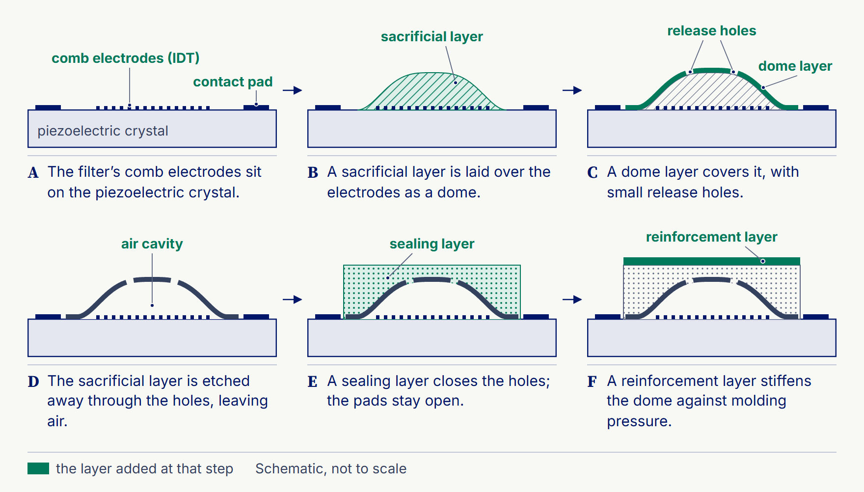
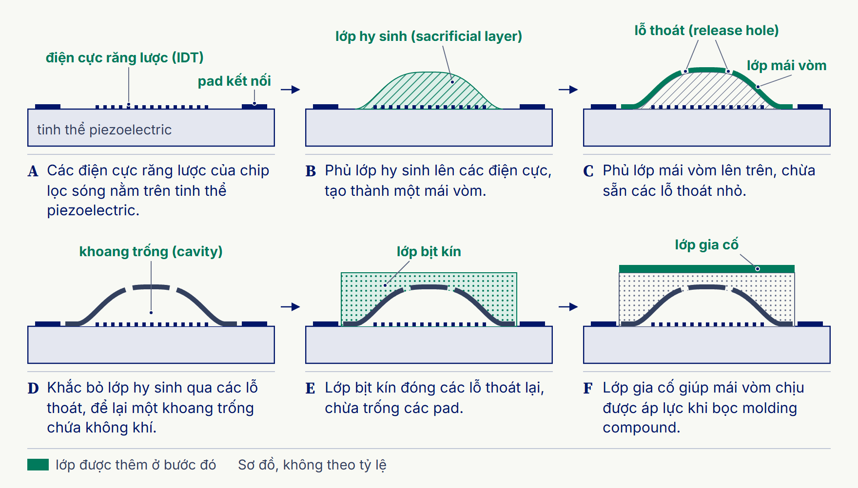
The dome starts as a mound: a sacrificial layer, laid over the comb electrodes only to be removed later. A dome layer is laid over the mound, with small release holes in it. The sacrificial layer is then etched away through the holes, leaving an air cavity under the dome. A sealing layer closes the holes, leaving open only the pads where the solder balls will go, and a second layer reinforces the dome.5.1
Mái vòm bắt đầu từ một “ụ” nhỏ: một lớp hy sinh (sacrificial layer) được phủ lên các điện cực răng lược, chỉ để sau đó bị loại bỏ. Kế đến là một lớp mái vòm phủ lên ụ ấy, chừa sẵn những lỗ thoát nhỏ. Lớp hy sinh sau đó bị khắc bỏ qua các lỗ thoát, để lại khoang trống chứa không khí bên dưới mái vòm. Một lớp bịt kín đóng các lỗ lại, chỉ chừa trống các pad sẽ gắn bi hàn, rồi một lớp thứ hai gia cố cho mái vòm.5.1
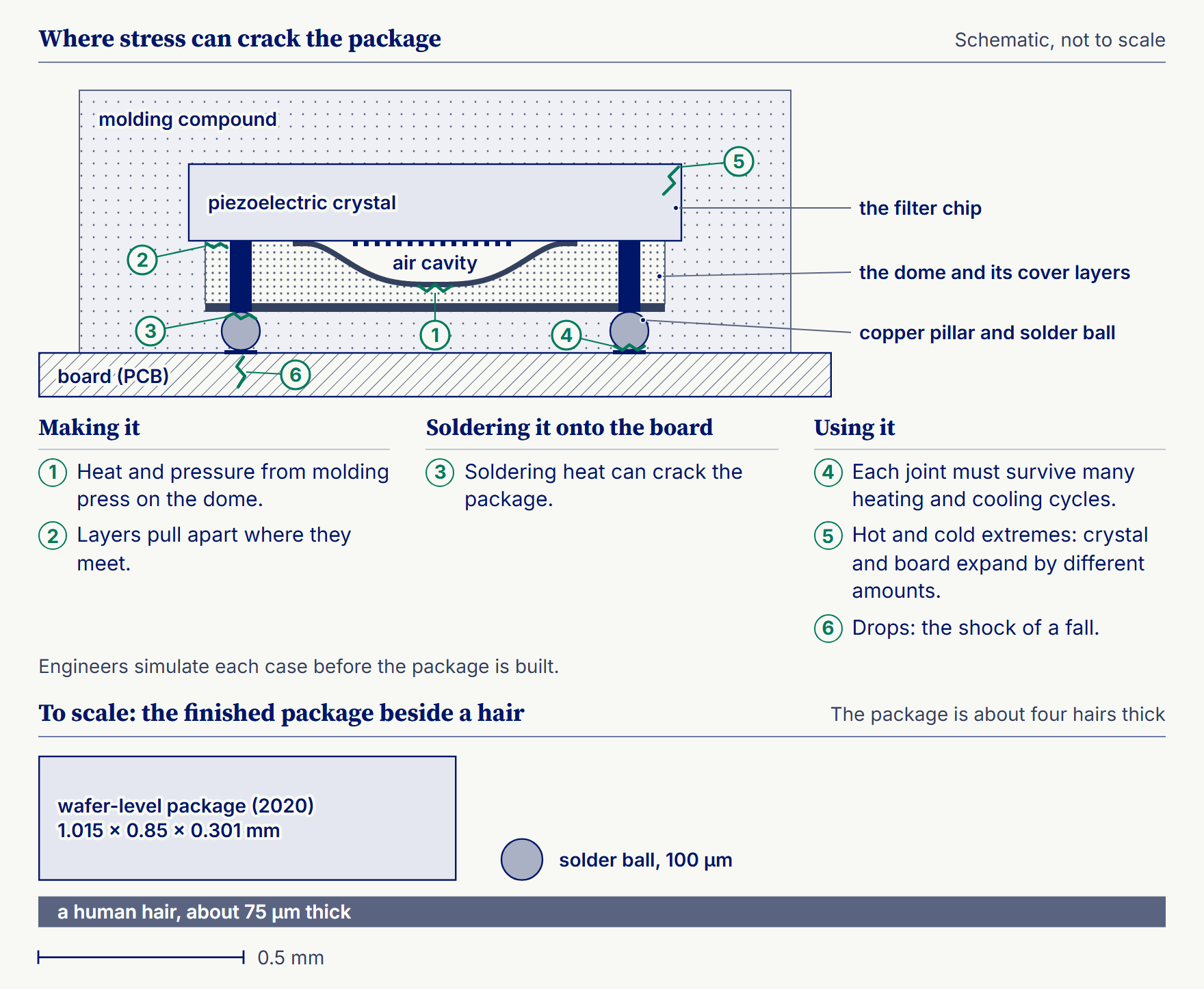
The reinforcement is there for a later step. Once the filter is mounted, molding compound is pressed around it, hot and under pressure, and the dome must not cave in. In one study, caps 20 and 45 µm thick collapsed under molding at 9 MPa and 175 °C, a pressure nearly 90 times that of the air around us.5.1
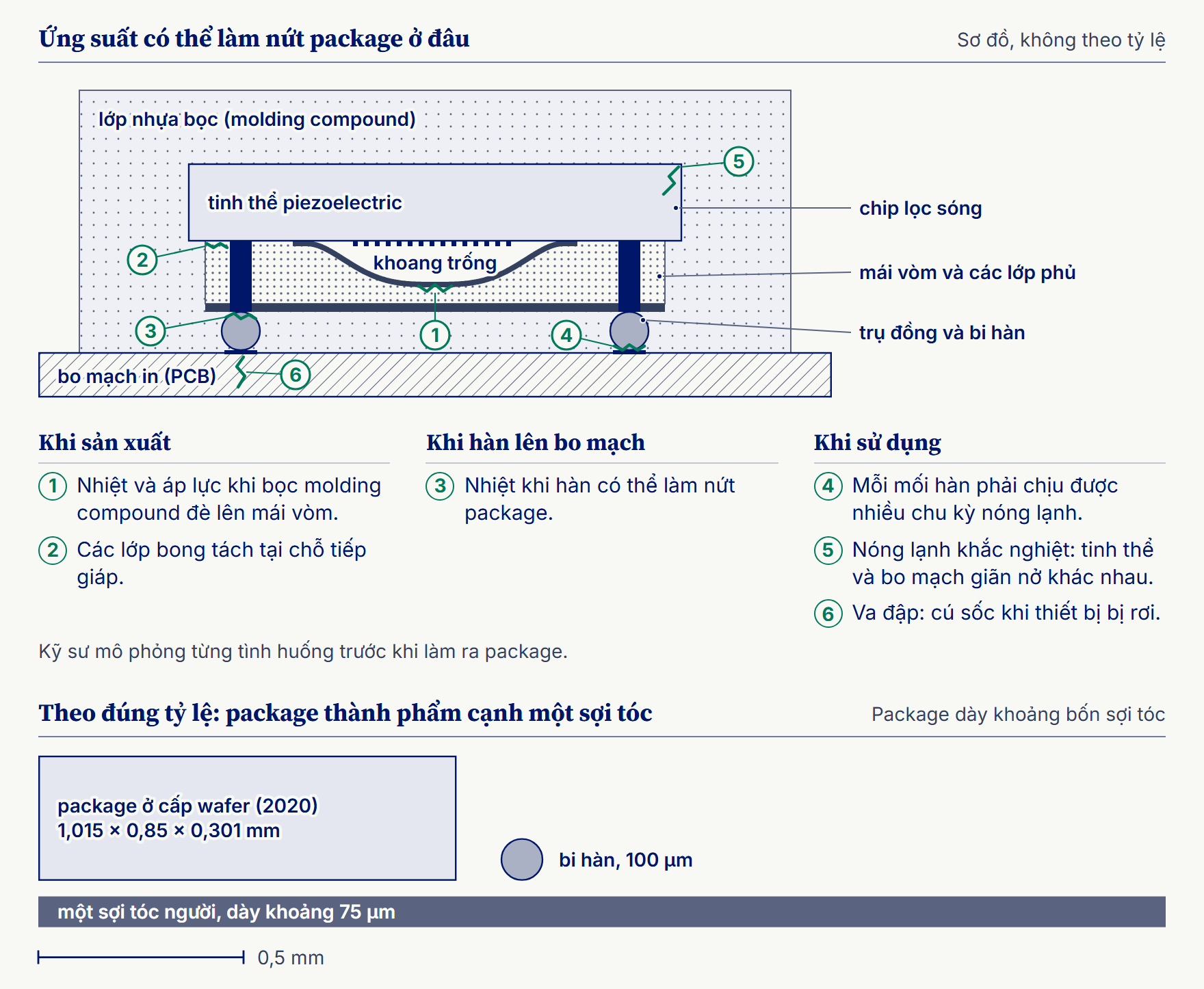
Lớp gia cố là để chuẩn bị cho một bước về sau. Sau khi chip lọc sóng được gắn xuống, lớp nhựa bọc được ép quanh nó ở nhiệt độ cao và áp suất lớn, và mái vòm không được sụp. Trong một nghiên cứu, những mái vòm dày 20 và 45 µm đã sụp khi bọc nhựa ở 9 MPa và 175 °C. Áp suất ấy gần gấp 90 lần áp suất không khí quanh ta.5.1
Materials are chosen and stress is simulated for the chip's whole life
Vật liệu được chọn và ứng suất được mô phỏng cho cả vòng đời con chip
A package like this is a stack of thin layers of different materials pressed tight together: crystal, metal, dome layers, solder, molding compound and, under it all, the board. Each expands by its own amount when it is heated, a mismatch in their coefficients of thermal expansion (CTE). Heated and cooled again during manufacture, layers bonded together pull against each other; the stress bends them, peels them apart where they meet and cracks them. So the materials are chosen to expand by similar amounts and to stick firmly to one another.
Một package như thế là một chồng nhiều lớp mỏng bằng những vật liệu khác nhau ép sát vào nhau: tinh thể, kim loại, các lớp mái vòm, thiếc hàn, lớp nhựa bọc và, dưới cùng, bo mạch. Khi bị nung nóng, mỗi vật liệu giãn nở một mức khác nhau, hiện tượng gọi là chênh lệch hệ số giãn nở nhiệt (CTE mismatch). Qua những lần nung lên rồi nguội xuống trong sản xuất, các lớp dính liền nhau kéo căng lẫn nhau; ứng suất ấy làm chúng cong, bong tách ở chỗ tiếp giáp và nứt. Vì vậy vật liệu phải được chọn sao cho chúng giãn nở gần như nhau và bám chặt vào nhau.
A given material may come from only a few suppliers. A development team gathers candidates, brings samples back and compares them, in simulation and in tests, before choosing.
Mỗi loại vật liệu như thế có khi chỉ vài nhà cung cấp làm ra. Nhóm phát triển tìm vật liệu ứng viên, nhận mẫu về rồi so sánh với nhau bằng mô phỏng và thử nghiệm trước khi chọn.
Simulation then predicts, before anything is built, how the design will fare over the chip’s whole life, in three stages (the plate below). Making it: heat and molding pressure bear on the dome, and layers can pull apart where they meet. Soldering it onto the board: the solder is melted again, one more round of heat the package must survive. Using it: a filter in a car may sit in freezing cold or great heat, so each solder joint must survive many cycles of heating and cooling, and phones get dropped. At each stage the model is asked where a crack could start, in the dome, where two layers meet, at a solder joint, at a corner of the crystal or in the board, and whether the filter’s signal still comes through cleanly; tests on finished parts then confirm what the model predicts. That is reliability: the chip must keep working for its whole life, not only on the day it is made.
Mô phỏng sau đó dự báo, trước khi làm thật, thiết kế sẽ chịu đựng ra sao qua trọn vòng đời con chip, theo ba giai đoạn (hình dưới đây). Lúc sản xuất: nhiệt và áp lực của lớp nhựa bọc đè lên mái vòm, các lớp có thể bong tách ở chỗ tiếp giáp. Lúc hàn lên bo mạch: thiếc hàn lại bị nung chảy, thêm một lần nóng nữa mà package phải chịu được. Lúc sử dụng: chip lọc sóng trong ô tô có thể gặp giá rét hay nắng nóng gay gắt, nên mỗi mối hàn phải chịu được nhiều chu kỳ nóng lạnh, còn điện thoại thì bị đánh rơi. Ở mỗi giai đoạn, mô hình phải trả lời vết nứt có thể bắt đầu ở đâu, trong mái vòm, ở chỗ hai lớp tiếp giáp, ở mối hàn, ở góc tinh thể hay trong bo mạch, và tín hiệu qua chip lọc sóng có còn sạch hay không; sau đó, các phép thử trên sản phẩm thật sẽ xác nhận điều mô hình dự báo. Đó chính là độ tin cậy: con chip phải chạy được suốt vòng đời, chứ không chỉ vào ngày xuất xưởng.
How small the finished package is
Package hoàn chỉnh nhỏ đến mức nào
The 2020 wafer-level package measures about 1.0 × 0.85 mm, and at about 0.3 mm it is about four hairs thick, a human hair being about 75 µm, as chapter 2 notes.5.1 Thin-film filter packages are among the thinnest made for mounting straight onto a phone’s radio module. The finished filter is a small block with solder balls on one face, soldered face down onto the board; inside, the dome still keeps the air over the combs. Solder balls are small too: in one 2002 filter package, set face down on a ceramic base, they were 100 µm across, a little thicker than a hair.5.1
Package ở cấp wafer năm 2020 có kích thước khoảng 1,0 × 0,85 mm và dày khoảng 0,3 mm, chừng bốn sợi tóc người.5.1 Như chương 2 đã nêu, mỗi sợi tóc dày khoảng 75 µm. Package màng mỏng của chip lọc sóng thuộc loại mỏng nhất để gắn thẳng lên module vô tuyến của điện thoại. Chip lọc sóng hoàn chỉnh là một khối nhỏ, một mặt mang các bi hàn, úp mặt xuống và hàn lên bo mạch; bên trong, mái vòm vẫn giữ khoảng khí phía trên các răng lược. Bi hàn cũng nhỏ: trong một package chip lọc sóng năm 2002, úp mặt xuống một nền gốm, bi hàn có đường kính 100 µm, nhỉnh hơn sợi tóc một chút.5.1
From 1996 to 2020 the filter’s package went from a ceramic box 5 mm square and 1.35 mm tall to a wafer-level package about 1 mm long and 0.3 mm thick. One requirement, a surface nothing may touch, set the package’s shape; the shape set the steps of the process; the steps set the materials; and simulation predicted how the design would fare over the chip’s whole life. Such filters now sit by the dozen on a smartphone’s radio board, and in cars too.
Từ 1996 đến 2020, package của chip lọc sóng đã đi từ chiếc hộp gốm vuông 5 mm, cao 1,35 mm, đến một package ở cấp wafer dài khoảng 1 mm và chỉ dày 0,3 mm. Một yêu cầu duy nhất, bề mặt không được để thứ gì chạm vào, quyết định hình dạng của package; hình dạng quyết định các bước làm; các bước quyết định vật liệu; còn mô phỏng dự báo thiết kế sẽ chịu đựng ra sao qua trọn vòng đời con chip. Giờ đây, những chip lọc sóng như thế nằm hàng chục con trên bo mạch vô tuyến của một chiếc điện thoại thông minh, và trong cả ô tô.
Could an RF filter go inside a 2.5D or 3D package?Chip lọc sóng có thể nằm bên trong một package 2.5D hay 3D không?
It can, in one form: a BAW filter can be sealed under a silicon cap wafer bonded on top and wired through with through-silicon vias (TSVs, chapter 7), and one design put active circuits on that cap, stacking a chip right on the filter.5.1 Whatever the package, a SAW filter’s working surface must face an empty cavity, because its wave travels along that surface, so it is packaged around that gap first, as in this chapter’s dome.5.1 In phones, filters are made as separate chips and set beside the others: premium phones use small modules holding several SAW filters in one compact package, Murata notes,5.8 and in one 2024 design of a phone’s radio front end, SAW filters and a switch, made in different processes, are mounted as separate chips side by side on one compact substrate: a system-in-package, chapter 4’s way of putting many parts in one package.5.9 2.5D and 3D packages, which join chips through far denser connections, are the subject of chapters 6 and 7.
Có thể, theo một cách: chip lọc sóng BAW có thể được bịt kín dưới một tấm nắp wafer silicon hàn lên trên, đi dây xuyên qua bằng các TSV (through-silicon via) (chương 7), và một thiết kế đã đặt mạch tích cực ngay trên tấm nắp ấy, tức xếp một con chip chồng thẳng lên chip lọc sóng.5.1 Dù package thế nào, bề mặt làm việc của chip lọc sóng SAW cũng phải hướng vào một khoang trống, vì sóng chạy dọc chính bề mặt ấy, nên trước hết nó được đóng gói quanh khoảng trống đó, như mái vòm trong chương này.5.1 Trong điện thoại, chip lọc sóng được làm thành những chip riêng rồi đặt cạnh các chip khác: theo Murata, điện thoại cao cấp dùng những module nhỏ gom nhiều chip lọc sóng SAW trong một package nhỏ gọn,5.8 và trong một thiết kế năm 2024 cho khối RF front-end (phần mạch vô tuyến nằm ngay sau ăng-ten) của điện thoại, các chip lọc sóng SAW và một chip chuyển mạch, làm bằng những quy trình khác nhau, là những chip riêng đặt cạnh nhau trên cùng một substrate nhỏ gọn: một system-in-package (SiP), cách gom nhiều linh kiện vào một package mà chương 4 đã kể.5.9 Package 2.5D và 3D, nơi các chip nối với nhau qua những kết nối dày đặc hơn nhiều, là chủ đề của chương 6 và chương 7.