Chapter 2 of 10Chương 2/10 6 min6 phút
What a package does, and how it is madeĐóng gói chip để làm gì và gồm những bước nào
A finished wafer holds many copies of one chip, and none of them can go into a phone yet. Each is a die: a bare sliver of silicon as brittle as glass, with contact pads far too small and too close together to solder to a circuit board. Packaging turns it into something a board can use. The package protects the die, feeds it power, carries its signals and takes away its heat, and on a simple chip it is made in nine main steps, from grinding the wafer thin to testing the finished part.
Một wafer đã chế tạo xong mang nhiều con chip giống hệt nhau, nhưng chưa con nào lắp được vào điện thoại. Mỗi con chip ấy là một die: một mảnh silicon trần giòn như thủy tinh, với những điểm tiếp xúc (pad) quá nhỏ và quá sát nhau để hàn thẳng lên bo mạch. Đóng gói chip biến nó thành thứ bo mạch dùng được. Một package (phần đóng gói của chip) bảo vệ die, cấp điện, dẫn tín hiệu và đưa nhiệt ra ngoài; với một con chip đơn giản, nó được làm qua chín bước chính, từ mài mỏng wafer đến kiểm thử thành phẩm.
In this chapter
Trong chương này
- The four jobs every package does
- How a die reaches a circuit board in three levels
- The nine steps that turn a finished wafer into a tested chip
- What sets advanced packaging apart from traditional packaging
- Bốn việc mà package nào cũng phải làm
- Die đi đến bo mạch qua ba cấp như thế nào
- Chín bước biến wafer thành những con chip đã kiểm thử
- Đóng gói tiên tiến khác đóng gói truyền thống ở đâu
Four jobs every package must do
Bốn việc mà package nào cũng phải đảm nhận
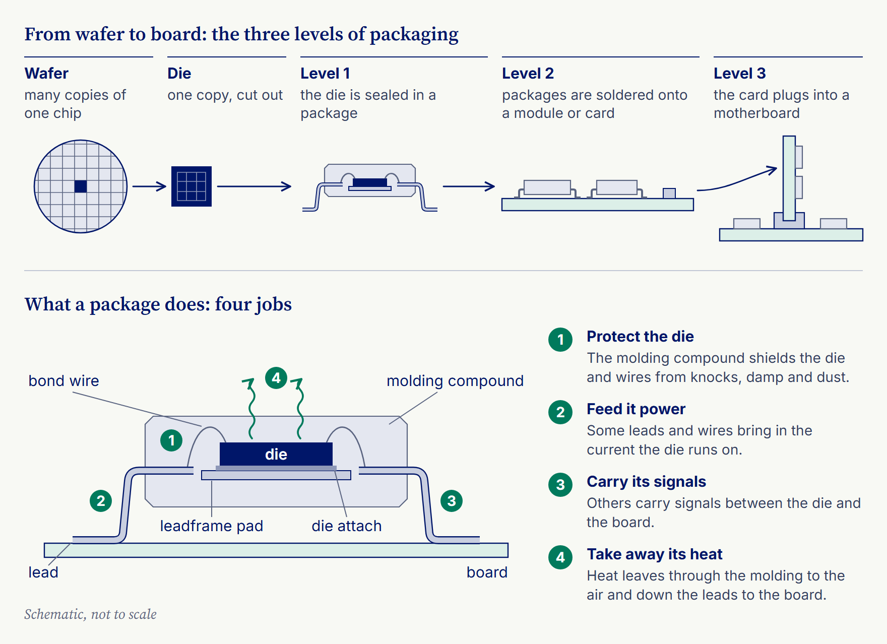
A textbook chapter on microelectronics packaging lists what a package must provide: signal distribution, heat dissipation, power distribution, and support and protection for the chip.2.1 In plainer words, it has four jobs (plate 2.1):
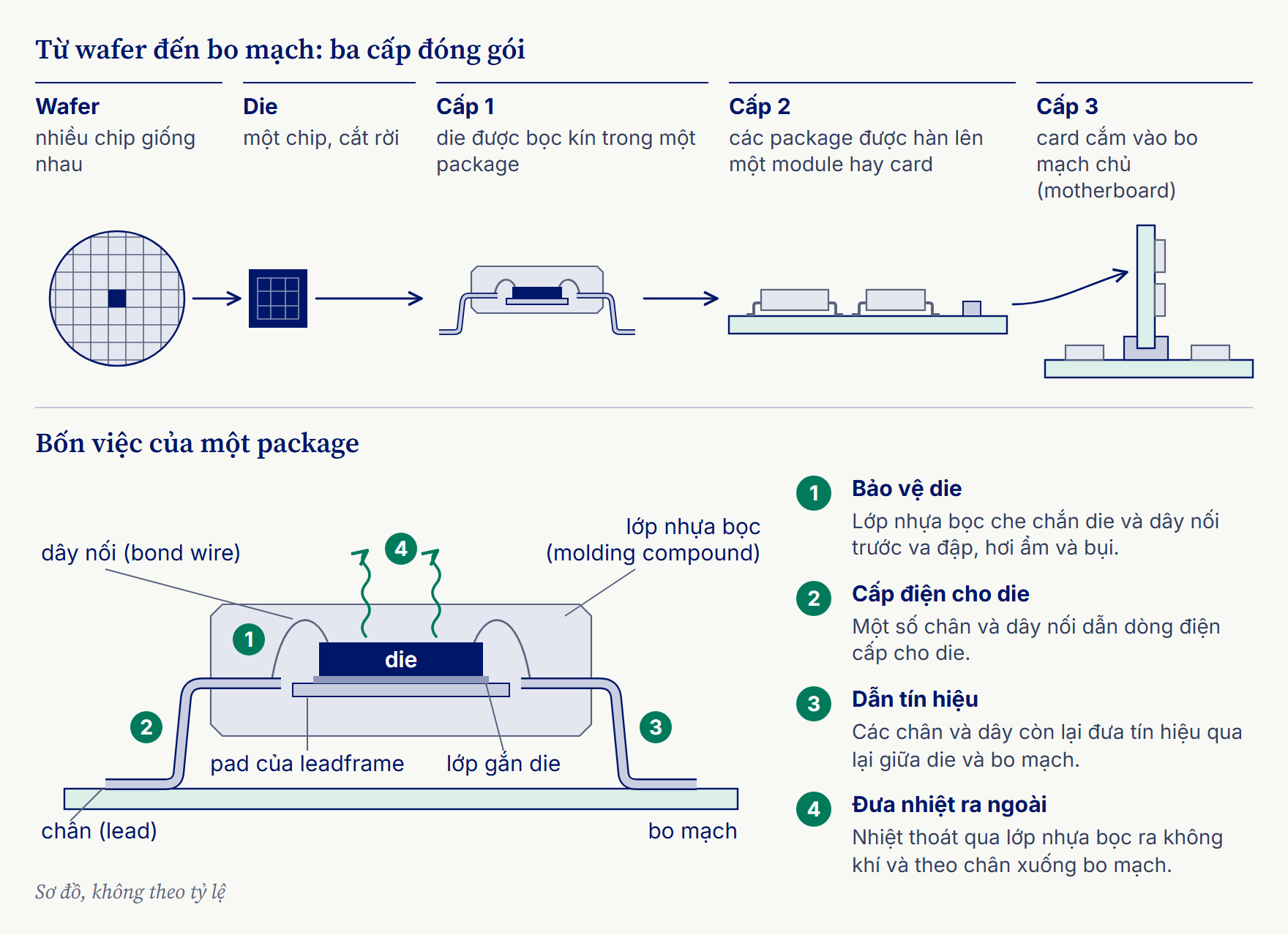
Một giáo trình về đóng gói vi điện tử liệt kê những gì package phải đảm bảo: phân phối tín hiệu, tản nhiệt, phân phối điện năng, đỡ và bảo vệ con chip.2.1 Nói gọn lại, package có bốn việc (hình 2.1):
- Protect the die. Silicon is brittle, and damp and dirt would corrode the metal on its surface, so the package encloses the die, shields it from knocks, moisture and dust, and holds it steady for years. How well it keeps doing that through heat, cold and damp is its reliability.
- Feed it power. A processor’s billions of transistors draw current in sudden surges as they switch, and the package must bring that current in steadily, with as little loss and as little drop in voltage as possible: its power delivery.
- Carry its signals. Every input and output (I/O) passes through the package, and fast signals must arrive clean, with as little noise and delay as possible.
- Take away its heat. A working chip turns almost all the power it draws into heat, and the faster it works, the more heat it gives off. The package has to carry that heat away before the die slows down or fails; this is its thermal management.
- Bảo vệ die. Silicon rất giòn, còn hơi ẩm và bụi bẩn có thể ăn mòn lớp kim loại trên bề mặt, nên package bọc lấy die, che chắn nó trước va đập, hơi ẩm và bụi, và giữ nó ổn định trong nhiều năm. Mức độ package giữ vững vai trò ấy qua nóng, lạnh và ẩm ướt được gọi là độ tin cậy.
- Cấp điện. Hàng tỷ bóng bán dẫn (transistor) của một bộ xử lý tiêu thụ dòng điện theo từng đợt tăng vọt khi chuyển mạch, và package phải đưa dòng điện ấy vào một cách ổn định, với hao hụt và sụt áp ít nhất có thể. Đó là việc power delivery (cấp nguồn).
- Dẫn tín hiệu. Mọi tín hiệu I/O (vào/ra) đều đi qua package, và tín hiệu tốc độ cao phải đến nơi nguyên vẹn, ít nhiễu và ít trễ nhất có thể.
- Đưa nhiệt ra ngoài. Con chip đang chạy biến gần như toàn bộ điện năng nó tiêu thụ thành nhiệt, và chip càng chạy nhanh càng tỏa nhiều nhiệt. Package phải dẫn lượng nhiệt ấy đi trước khi die chậm lại hoặc hỏng; đó là việc quản lý nhiệt.
A chip reaches the board in three levels
Con chip đi từ die đến bo mạch qua ba cấp
Engineers describe the trip from die to finished product in three levels (plate 2.1). At level 1, the die is sealed in a package: one die in a single-chip package, or two or more in a multi-chip package. At level 2, packages are soldered onto a module or card, a printed circuit board (PCB) that joins them. At level 3, the card plugs into a motherboard. Packaging, in this book, means level 1, where the die meets the outside world.
Giới kỹ thuật chia hành trình từ die đến sản phẩm hoàn chỉnh thành ba cấp (hình 2.1). Ở cấp 1, die được bọc kín trong một package: một die trong package đơn chip, hoặc từ hai die trở lên trong package đa chip. Ở cấp 2, các package được hàn lên một module hoặc card, tức một tấm bo mạch in (PCB) nối chúng với nhau. Ở cấp 3, card được cắm vào bo mạch chủ. Trong cuốn sách này, đóng gói chip là cấp 1, nơi die gặp thế giới bên ngoài.
Inside the package, the die usually sits on one of two bases. In simple packages it is glued to a leadframe, a thin metal frame whose fingers become the package’s leads, the metal legs that are soldered to the board. In many others it sits on a substrate, a small multilayer circuit board that spreads the die’s tightly packed connections out to wider-spaced solder balls or flat contacts underneath, and carries the die’s signals and power out to the board.
Bên trong package, die thường nằm trên một trong hai loại giá đỡ. Ở những package đơn giản, die được dán lên một leadframe (khung chân kim loại), tức một khung kim loại mỏng có các nhánh sẽ trở thành chân của package, những chân kim loại được hàn xuống bo mạch. Ở nhiều package khác, die nằm trên một substrate (đế), tức một tấm mạch nhỏ nhiều lớp. Substrate dàn các điểm nối dày đặc của die ra những bi hàn hoặc điểm tiếp xúc phẳng thưa hơn ở mặt dưới, và dẫn tín hiệu cùng điện năng của die ra bo mạch.
How a finished wafer becomes a tested chip
Wafer đã chế tạo xong thành chip đã kiểm thử ra sao
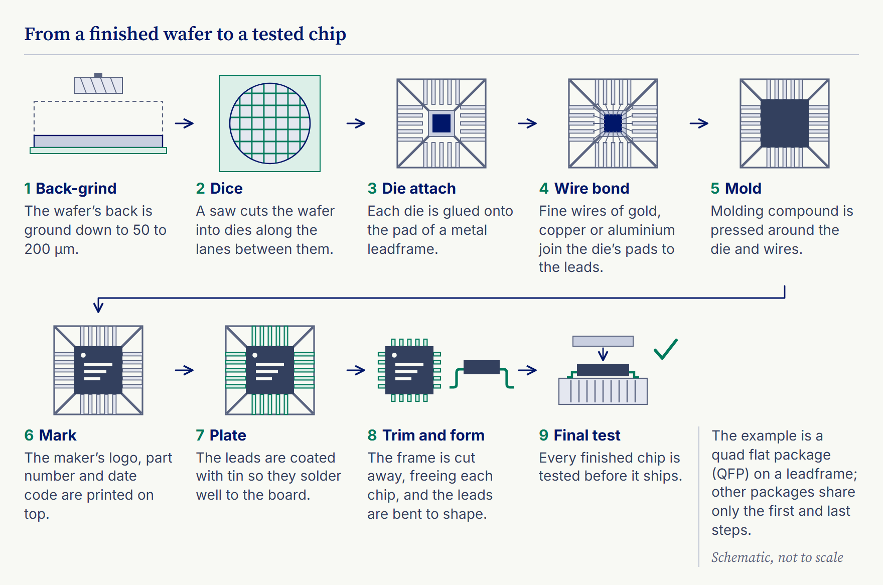
Turning a finished wafer into tested chips takes nine steps for one simple package, a quad flat package (QFP) on a leadframe (plate 2.2); other packages share the first and last of them but join and protect the die in other ways (chapters 4 and 5). The work is called assembly, and it starts with the wafer itself. By then the wafer’s dies have usually been tested with fine probes, and the failures noted on a map of the wafer so that they are not packaged; chapter 8 says more about that testing.2.2
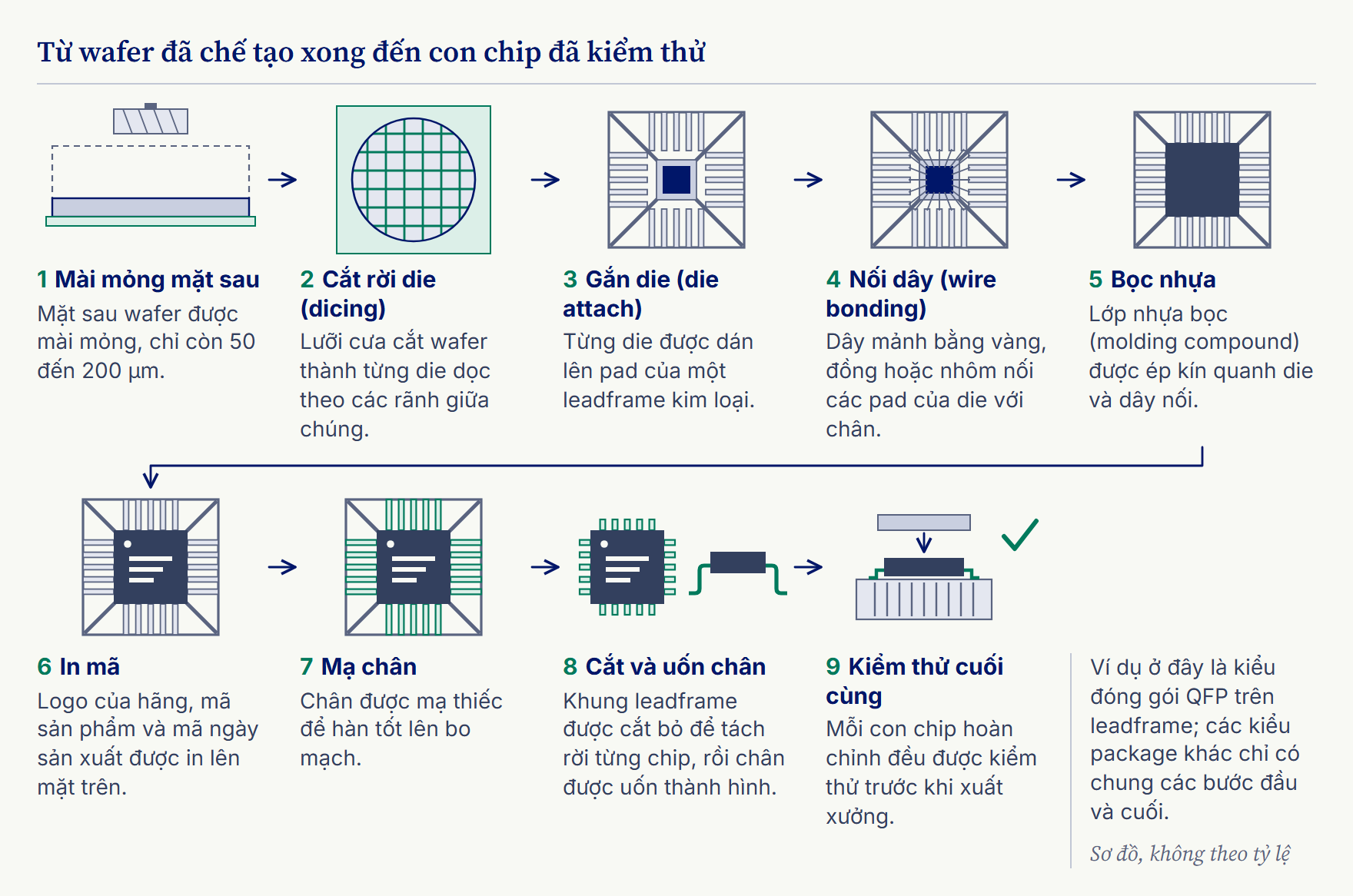
Với một package đơn giản, kiểu đóng gói QFP (Quad Flat Package) trên leadframe, wafer đã chế tạo xong phải qua chín bước mới thành những con chip đã kiểm thử (hình 2.2). Các kiểu package khác cũng có những bước đầu và cuối ấy, nhưng nối và bảo vệ die theo cách khác (chương 4 và 5). Công việc này được gọi là lắp ráp, và nó bắt đầu từ chính tấm wafer. Đến lúc ấy, các die trên wafer thường đã được kiểm thử bằng những đầu dò rất mảnh, và die hỏng được ghi lại trên bản đồ wafer để không bị đem đi đóng gói; chương 8 sẽ nói thêm về việc kiểm thử này.2.2
A 300 mm wafer is nominally 775 µm thick, about ten human hairs side by side (a hair is about 75 µm across, though hairs vary widely).2.3, 2.4 That is much thicker than a package needs, so first the back of the wafer is ground away, a step called back-grinding, often to about 200 µm, and in some cases to 50 µm or less, from under three hairs to under one.2.5 A thinner die makes a thinner package, but it is also easier to break in handling.
Một wafer 300 mm dày danh định 775 µm, cỡ mười sợi tóc người đặt cạnh nhau (một sợi tóc dày khoảng 75 µm, dù tóc mỗi người mỗi khác).2.3, 2.4 Như thế là dày hơn nhiều so với mức package cần, nên trước hết mặt sau wafer được mài bớt, bước gọi là mài mỏng mặt sau (back-grinding). Wafer thường được mài xuống khoảng 200 µm, có khi 50 µm hoặc mỏng hơn, tức từ chưa đầy ba sợi tóc còn chưa tới một sợi.2.5 Die mỏng hơn thì package mỏng hơn, nhưng cũng dễ vỡ hơn khi thao tác.
Next, a saw cuts the wafer into dies along the narrow lanes left between them, a step called dicing. In die attach, each die is glued onto the die pad at the centre of a metal leadframe. Then wire bonding joins the bond pads on the die to the leads with fine wires;2.6 chapter 3 shows how those wires are laid. The die and its wires are then sealed in molding compound, a hard plastic pressed around them, which does the protecting.
Tiếp theo, một lưỡi cưa cắt wafer thành từng die dọc theo những rãnh hẹp chừa sẵn giữa chúng; bước này gọi là dicing (cắt wafer thành die). Ở bước die attach (gắn die), mỗi die được dán lên phần pad đỡ die ở giữa một leadframe kim loại. Sau đó, ở bước nối dây (wire bonding), những sợi dây rất mảnh nối các pad trên mặt die với chân;2.6 chương 3 sẽ cho thấy những sợi dây ấy được kéo ra sao. Rồi die và dây được bọc kín trong lớp nhựa bọc (molding compound), một loại nhựa cứng được ép quanh chúng, chính là phần bảo vệ die.
Four last steps finish the outside. The maker’s logo, part number and date code are marked on top, usually by laser; the leads are usually plated with tin so that they solder well to the board; and in trim and form, the frame is cut away and the leads are bent to shape. Until that cut, the chips on one strip of leadframe are still joined through the frame, which carries the plating current to every lead, so plating comes first and trim and form is where they finally come apart. Last comes final test: every finished chip is tested before it ships.
Bốn bước cuối hoàn thiện phần bên ngoài. Logo của hãng, mã sản phẩm và mã ngày sản xuất được in lên mặt trên, thường bằng laser; chân thường được mạ thiếc để hàn tốt lên bo mạch; rồi ở bước cắt và uốn chân (trim and form), khung bị cắt bỏ và chân được uốn thành hình. Trước nhát cắt ấy, các con chip trên cùng một dải leadframe vẫn dính liền với nhau qua khung, và khung dẫn dòng điện mạ tới từng chân, nên việc mạ diễn ra trước, và đến bước trim and form chúng mới thật sự tách rời. Cuối cùng là kiểm thử cuối cùng: mọi con chip thành phẩm đều phải qua kiểm thử trước khi xuất xưởng.
What separates traditional from advanced packaging
Đóng gói truyền thống khác đóng gói tiên tiến ở đâu
The package in plate 2.2 is traditional packaging: a single die, wired to its leads by methods in use for decades. Packages are usually sorted by how the die connects to them. Wire bonding joins pads around the die’s edge, as above. In flip chip, the die carries small bumps across its whole face and is turned face down so that they land on the package (chapter 4). In wafer-level packaging, the package’s wiring is built on a whole wafer at once, and the wafer is cut only at the end. In fan-in, that is the chip’s own uncut wafer; in fan-out, it is a new wafer made by setting already-cut dies in molding compound (chapter 5).
Package trong hình 2.2 thuộc loại đóng gói truyền thống: một die duy nhất, nối với chân bằng những phương pháp đã dùng hàng chục năm. Các kiểu đóng gói thường được phân loại theo cách die nối với package. Với kiểu nối dây, những sợi dây đi ra từ các pad nằm quanh mép die, như vừa thấy. Với flip chip, die mang những bump nhỏ trải khắp bề mặt và được lật úp để các bump ấy chạm xuống package (chương 4). Với wafer-level packaging (đóng gói ngay trên wafer), lớp dây dẫn của package được làm trên cả một tấm wafer cùng lúc, và wafer chỉ được cắt ở bước cuối. Ở kiểu fan-in, đó là chính wafer chưa cắt của con chip; ở kiểu fan-out, đó là một wafer mới, tạo thành từ các die đã cắt rời đặt trong lớp nhựa bọc (chương 5).
Advanced packaging, met in chapter 1, goes further: far denser connections and processes borrowed from the fab, such as depositing thin films and patterning fine wiring, at micrometre precision or finer. At its high end, several dies sit side by side or are stacked in one package. It builds on traditional packaging, which carries on beside it. Chapter 3 begins at the traditional end, with the first metal cans.
Đóng gói tiên tiến (advanced packaging), đã gặp ở chương 1, đi xa hơn: mối nối dày đặc hơn nhiều và các quy trình mượn từ nhà máy sản xuất chip (fab), như lắng đọng màng mỏng và tạo hình những đường dây dẫn mảnh, ở độ chính xác micromet hoặc cao hơn. Ở mức cao nhất, nhiều die được đặt cạnh nhau hoặc xếp chồng trong cùng một package. Đóng gói tiên tiến xây tiếp trên nền đóng gói truyền thống, và hai cách làm vẫn song hành. Chương 3 bắt đầu từ phía truyền thống, với những chiếc hộp kim loại đầu tiên.