Chapter 3 of 10Chương 3/10 8 min8 phút
From pins to solder balls: sixty years of chip packagesTừ chân cắm đến bi hàn: sáu mươi năm đóng gói chip
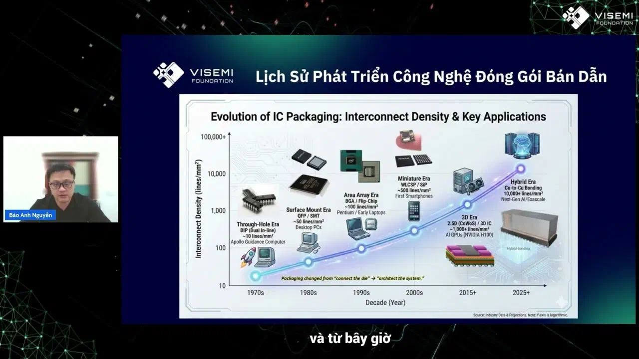
Chip packages have been reshaped, again and again, by one problem: each new kind of device needed more connections between its chips and the board than the last. The first packages ran a handful of leads out of a metal can. Later ones lined up dozens of pins along their edges, and when the edges ran out of room, the contacts moved to the underside as a grid of solder balls. Inside most of them, thin wires joined the die, the bare slice of silicon, to the package at its edge.
Package (phần đóng gói của chip) đã nhiều lần đổi dạng vì một bài toán duy nhất: mỗi thế hệ thiết bị mới lại cần nhiều kết nối giữa con chip và bo mạch hơn thế hệ trước. Những package đầu tiên chỉ đưa vài chân ra khỏi một chiếc hộp kim loại. Về sau, hàng chục chân được xếp dọc các mép, và khi mép hết chỗ, tiếp điểm chuyển xuống mặt dưới thành một lưới bi hàn. Bên trong phần lớn các package ấy, die, tức mảnh silicon trần, vẫn được nối ra ngoài bằng những sợi dây mảnh gắn ở mép.
Packaging is the work of sealing a die in such a package, which protects it and carries its signals, power and heat to the board. This chapter follows the package from the 1960s to the 2010s, the decades when most connections still left the die at its edge.
Đóng gói chip là công việc đặt die vào một package như thế để bảo vệ die, đồng thời dẫn tín hiệu, điện năng và nhiệt của nó ra bo mạch. Chương này đi theo package từ thập niên 1960 đến thập niên 2010, quãng thời gian mà phần lớn kết nối vẫn rời die từ mép.
In this chapter
Trong chương này
- How metal cans and flat-packs protected the first chips
- Why the DIP, with its two rows of pins, became the standard of the 1970s
- How thin wires join a die to its package
- How QFP and QFN packages crowded more contacts round the edge
- Why ball grids moved the contacts to the underside
- How packages shrank almost to the size of their chips and began to stack
- Hộp kim loại và flat-pack đã bảo vệ những con chip đầu tiên ra sao
- Vì sao kiểu đóng gói DIP với hai hàng chân trở thành tiêu chuẩn của thập niên 1970
- Những sợi dây mảnh nối die với package như thế nào
- Các kiểu đóng gói QFP và QFN đã dồn thêm tiếp điểm quanh mép ra sao
- Vì sao lưới bi hàn đưa tiếp điểm xuống mặt dưới
- Package đã thu nhỏ gần bằng con chip và bắt đầu xếp chồng lên nhau như thế nào
Metal cans and flat-packs open the story
Hộp kim loại và flat-pack mở đầu lịch sử đóng gói chip
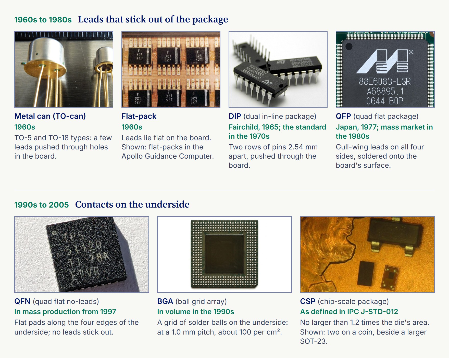
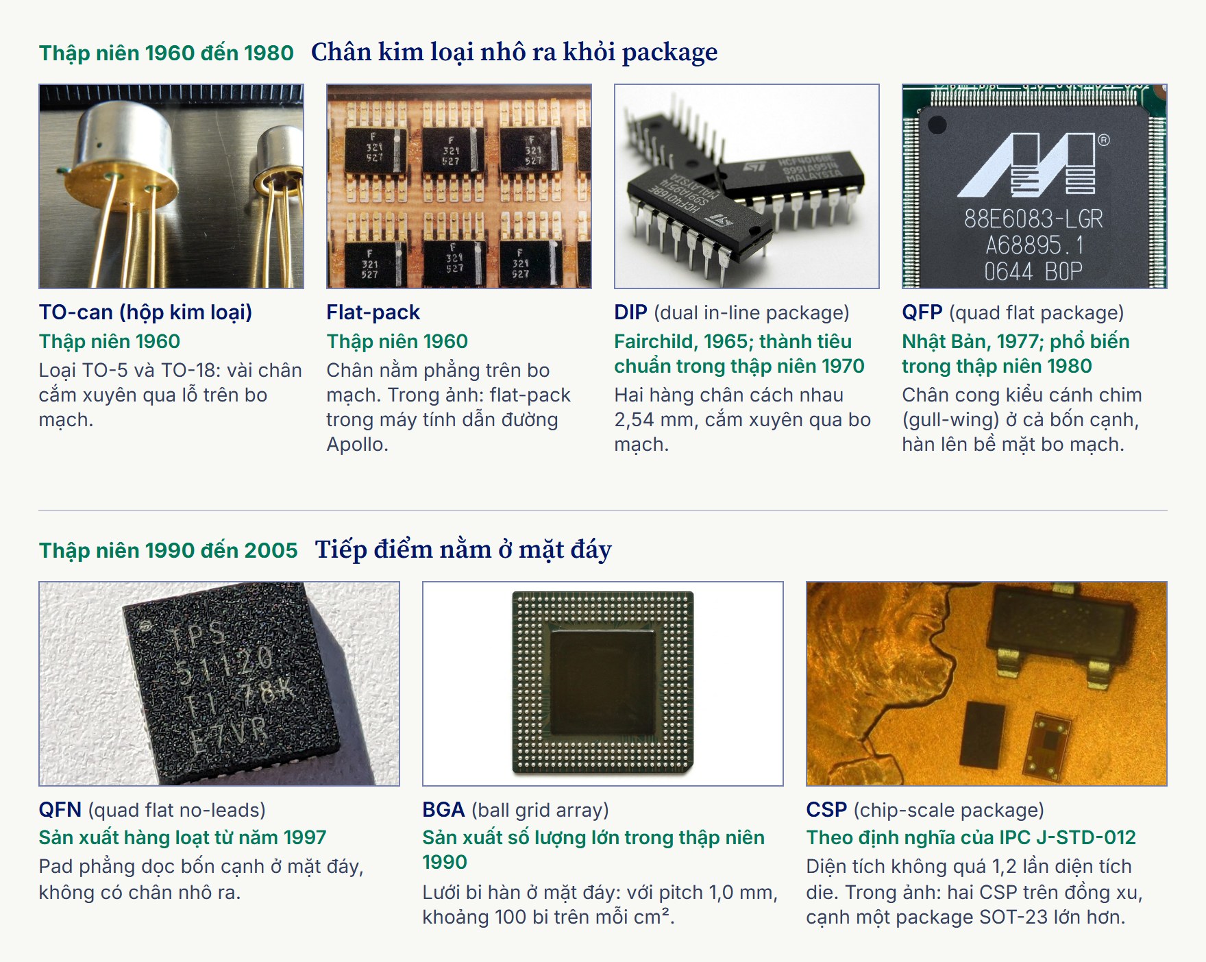
Through the 1960s, many transistors came in metal cans of the TO-5 and TO-18 types: a small round can with a few leads running out of its base and through holes in the circuit board. Fairchild’s first ICs went into such cans, fitted with up to ten leads.3.1 Such a can is a hermetic package. It is sealed airtight, so moisture and air are kept away from the costly chip inside.
Trong thập niên 1960, nhiều bóng bán dẫn (transistor) nằm trong TO-can (hộp kim loại) thuộc các loại TO-5 và TO-18. Đó là một hộp tròn nhỏ, vài chân kim loại chìa ra từ đáy và cắm xuyên qua các lỗ trên bo mạch. Những IC đầu tiên của Fairchild cũng nằm trong loại hộp ấy, sửa lại cho có tới mười chân.3.1 Hộp như vậy thuộc kiểu đóng gói kín: hộp được hàn kín khí, nên hơi ẩm và không khí không lọt tới được con chip đắt tiền bên trong.
The flat-pack brought the package down onto the board. Devised at Texas Instruments to take up as little board area as possible, it is a thin body whose leads lie flat on the board’s surface.3.1 Flat-packs went to the Moon: the Apollo Guidance Computers that flew there were built from thousands of integrated circuits (ICs) in flat-packs, each holding two logic gates; Fairchild designed that IC, and Philco made it.3.2, 3.3 These ceramic and metal packages protected their chips very well but cost more than plastic ones, and they served avionics and space programmes such as Apollo.3.1, 3.2
Flat-pack đưa package nằm áp xuống mặt bo mạch. Texas Instruments nghĩ ra nó để chiếm ít diện tích bo mạch nhất có thể: thân mỏng, các chân nằm phẳng trên mặt bo.3.1 Flat-pack từng bay tới Mặt Trăng: máy tính dẫn đường Apollo (Apollo Guidance Computer) trên những chuyến bay ấy được lắp từ hàng nghìn mạch tích hợp (IC) đóng gói kiểu flat-pack, mỗi flat-pack chứa hai cổng logic; loại IC này do Fairchild thiết kế và Philco sản xuất.3.2, 3.3 Những package gốm (ceramic package) và hộp kim loại như thế bảo vệ con chip rất tốt nhưng đắt hơn loại bằng nhựa, và được dùng trong điện tử hàng không và các chương trình không gian như Apollo.3.1, 3.2
The DIP rules the age of through-hole pins
Kiểu đóng gói DIP thống trị thời chân cắm xuyên lỗ
Commercial electronics needed something cheaper. In 1965 Fairchild devised the dual in-line package (DIP): the first was a 14-lead ceramic body with two rows of pins, 2.54 mm (0.1 inch) apart along each row.3.1, 3.4 Molded in plastic, it became cheap enough for almost any product: by the early 1970s most chips were packaged in low-cost plastic DIPs, and the DIP was the standard package of that decade.3.1, 3.5
Điện tử thương mại cần một giải pháp rẻ hơn. Năm 1965, Fairchild nghĩ ra kiểu đóng gói DIP (Dual In-line Package): chiếc đầu tiên là một thân gốm 14 chân xếp thành hai hàng, các chân cách nhau 2,54 mm (0,1 inch) dọc theo mỗi hàng.3.1, 3.4 Khi được đúc bằng nhựa, DIP rẻ tới mức dùng được cho gần như mọi sản phẩm: đến đầu thập niên 1970, phần lớn chip được đóng gói trong DIP nhựa giá rẻ, và DIP trở thành kiểu đóng gói tiêu chuẩn của cả thập niên ấy.3.1, 3.5
A DIP’s pins are through-hole: each is pushed through a hole drilled in the printed circuit board (PCB) and soldered on the far side. That holds the chip firmly, but every pin takes a hole through the whole board. With its pins 2.54 mm apart and only along its two long sides, a small DIP about 10 mm long carries four a side, eight in all.
Chân của DIP thuộc loại chân cắm xuyên lỗ (through-hole): mỗi chân được cắm qua một lỗ khoan trên bo mạch in (PCB) rồi hàn ở mặt bên kia. Cách này giữ con chip rất chắc, nhưng mỗi chân lại chiếm một lỗ xuyên suốt bo mạch. Với các chân cách nhau 2,54 mm và chỉ nằm dọc hai cạnh dài, một DIP nhỏ dài khoảng 10 mm chỉ có bốn chân mỗi bên, tổng cộng tám chân.
Thin wires join the die at its edge
Những sợi dây mảnh nối mép die với package
Inside the package, the die is joined to its pins by wire bonding. The die is glued face up onto a leadframe, a thin metal frame whose fingers become the pins, and its circuits end in small pads along its edge. In the most common method, a machine melts the end of a fine wire into a tiny ball, presses the ball onto a pad, draws the wire up and over in a loop, presses it down onto a finger of the leadframe, then moves to the next pad. Bond wires are made of gold, copper or aluminium, and sometimes silver.3.6 The die and its wires are then sealed in molding compound, a hard plastic, and the fingers left outside are trimmed and bent into pins.
Bên trong package, die được nối với các chân bằng nối dây (wire bonding). Die nằm ngửa, dán trên một leadframe (khung chân kim loại), tức một khung kim loại mỏng có các ngón về sau sẽ thành chân chip. Mạch điện của die kết thúc ở những điểm tiếp xúc (pad) nhỏ chạy dọc mép. Theo cách phổ biến nhất, máy nối dây nung chảy đầu một sợi dây mảnh thành một viên bi nhỏ, ấn viên bi lên một pad, kéo dây vồng lên thành vòng cung, ấn đầu kia xuống một ngón của leadframe, rồi chuyển sang pad kế tiếp. Dây nối làm bằng vàng, đồng hoặc nhôm, đôi khi bằng bạc.3.6 Sau đó, die cùng các sợi dây nằm kín trong lớp nhựa bọc (molding compound) cứng, còn phần ngón thò ra ngoài thì cắt gọn, uốn thành chân.
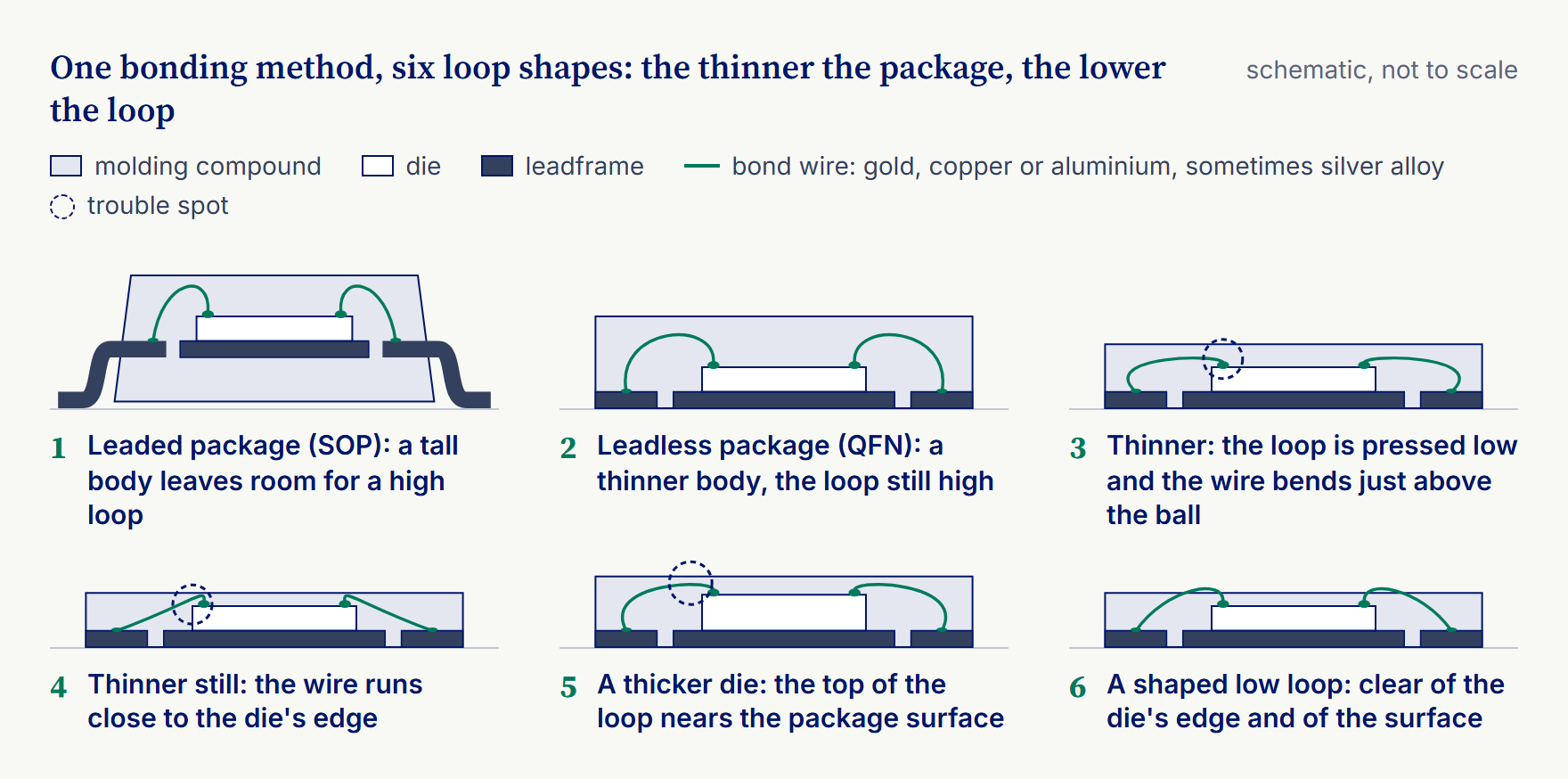
One machine can make many shapes of loop, and the shape matters more as packages get thinner. A tall leaded package leaves room for a high loop. In a thin one the loop must be pressed low, and the wire comes close to trouble: bent sharply just above the ball it starts from, running near the die’s edge, or rising too near the package surface (plate 3.2).
Cùng một máy có thể tạo ra nhiều dáng vòng dây, và dáng dây càng quan trọng khi package càng mỏng. Package có chân, thân cao, còn đủ chỗ cho vòng dây cao. Trong package mỏng, vòng dây phải ép thấp, và sợi dây dễ gặp sự cố: bị gập gắt ngay trên viên bi nơi dây bắt đầu, chạy sát mép die, hoặc vồng lên quá gần mặt trên package (hình 3.2).
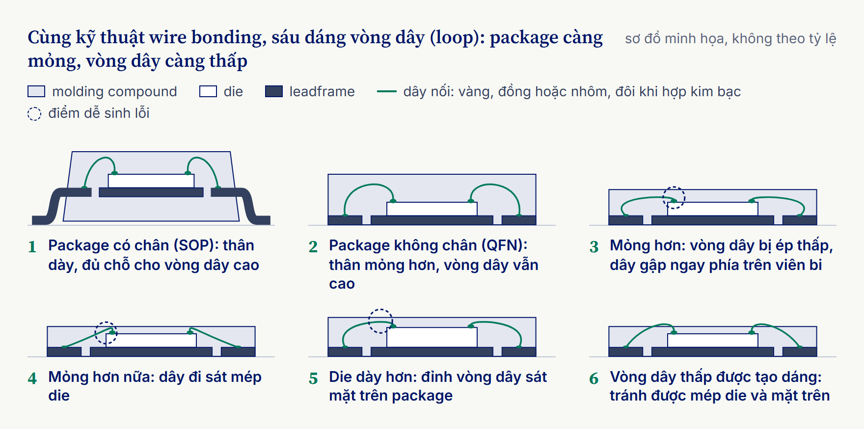
No loop shape fixes wire bonding’s real limit: the wires start from pads along the die’s edge, in one row or a few staggered ones, so a die’s connections grow with its perimeter, not with its area. Wire bonding is still in wide use, for chips that need fewer connections and for stacks of memory dies wired one above another; chapter 4 follows the way round the limit.
Không dáng vòng dây nào khắc phục được giới hạn thật sự của nối dây: dây bắt đầu từ các pad dọc mép die, xếp thành một hàng hoặc vài hàng so le, nên số kết nối của die tăng theo chu vi chứ không theo diện tích. Wire bonding vẫn được dùng rộng rãi, cho những con chip cần ít kết nối và cho các chồng die bộ nhớ nối dây tầng này trên tầng kia; chương 4 sẽ đi theo lối vượt qua giới hạn này.
QFP and QFN crowd more contacts round the edge
Kiểu đóng gói QFP và QFN dồn thêm tiếp điểm quanh mép
By the 1980s personal computers, the IBM PC among them (August 1981), had put chips on desks, and each chip did more work, so it needed more pins.3.7 Boards were also filling up with parts on both faces, where holes drilled right through get in the way. The answer was surface-mount technology (SMT): a package’s leads are soldered onto pads on the board’s surface instead of passing through it. The small outline package (SOP) kept two rows of leads, bent to sit on the surface. The quad flat package (QFP), first made in Japan in 1977 as a plastic package for calculator chips, ran leads out of all four sides.3.5
Đến thập niên 1980, máy tính cá nhân, trong đó có chiếc IBM PC (tháng 8/1981), đã đưa chip lên bàn làm việc. Mỗi con chip phải gánh nhiều việc hơn, nên cần nhiều chân hơn.3.7 Bo mạch cũng ngày càng chật linh kiện ở cả hai mặt, khiến những lỗ khoan xuyên suốt bo trở thành vật cản. Lời giải là Surface Mount Technology (SMT, gắn linh kiện lên bề mặt bo mạch): chân của package được hàn lên các pad trên mặt bo thay vì cắm xuyên qua bo. Kiểu đóng gói SOP (Small Outline Package) vẫn giữ hai hàng chân, nhưng chân được uốn để đặt lên bề mặt. Kiểu đóng gói QFP (Quad Flat Package), ra đời ở Nhật Bản năm 1977 dưới dạng package nhựa cho chip máy tính bỏ túi, đưa chân ra cả bốn cạnh.3.5
A QFP’s leads can sit 0.5 mm apart, five times closer than a DIP’s pins: a low-profile QFP 10 mm square carries 64 of them.3.8 The quad flat no-lead (QFN) package, in mass production from 1997, cut the leads back to pads on the underside of the package.3.9 As the word quad in its name says, those pads still sit along its four sides.
Chân của QFP có thể cách nhau 0,5 mm, sát hơn chân DIP năm lần: một QFP mỏng cỡ 10 × 10 mm mang 64 chân.3.8 Kiểu đóng gói QFN (Quad Flat No-lead), sản xuất hàng loạt từ năm 1997, cắt cụt chân thành những pad ở mặt dưới của package.3.9 Như chữ quad trong tên gọi cho biết, các pad ấy vẫn xếp dọc bốn cạnh của package.
Both still bring every connection to the edge, and an edge grows only with a package’s width. Double the width and the edge doubles, but the area underneath grows four times.
Dù vậy, cả hai vẫn dồn mọi kết nối ra mép, mà chiều dài mép chỉ tăng theo bề rộng của package. Bề rộng tăng gấp đôi thì mép cũng chỉ dài gấp đôi, trong khi diện tích mặt dưới tăng gấp bốn.
Ball grids use the underside
Lưới bi hàn tận dụng cả mặt dưới của package
Laptops, and then mobile phones, needed chips with still more connections in less board space, and the edge could no longer hold them. The way out was to use the underside, an area array of contacts. Pins had moved there first: the pin grid array (PGA), developed in Japan in 1975 for mainframe computers, set 52 pins, and later many more, in a grid across its underside.3.5 In a ball grid array (BGA) the die sits on a substrate, a small multilayer circuit board, and the substrate’s underside carries a grid of solder balls that melt onto matching pads on the board. Ball grid arrays came into wide use in the 1990s, and versions with more closely spaced balls went into phones.3.9
Máy tính xách tay rồi điện thoại di động đòi chip có nhiều kết nối hơn nữa trên diện tích bo mạch nhỏ hơn, và mép package không còn đủ chỗ. Lối ra là dùng mặt dưới của package, tức area array (tiếp điểm trải khắp mặt dưới). Chân cắm đã chuyển xuống đó trước: kiểu đóng gói PGA (pin grid array), ra đời ở Nhật Bản năm 1975 cho máy tính lớn (mainframe), xếp 52 chân, về sau nhiều hơn hẳn, thành một lưới trên khắp mặt dưới.3.5 Trong kiểu đóng gói BGA (ball grid array), die nằm trên một substrate (đế), tức một tấm mạch nhỏ nhiều lớp, và mặt dưới của substrate mang một lưới bi hàn; khi nung chảy, các bi hàn dính vào những pad tương ứng trên bo mạch. BGA được dùng rộng rãi từ thập niên 1990, và những bản có bi hàn xếp sát hơn được dùng nhiều trong điện thoại.3.9
The balls can be set 1.0 mm apart, among the wider spacings in use; this spacing is called the pitch, and at 1.0 mm a square centimetre holds about 100 of them.3.10 That is twice the QFP’s spacing, yet the grid wins: on a 10 mm square it holds 100 balls, more than the edge of the same square can take even at 0.5 mm. Chapter 7 carries the count down to today’s finest connections. Inside, the die may still be wire-bonded to its substrate; what changed is that the package now meets the board across its underside, not only at its edge.
Các bi hàn có thể cách nhau 1,0 mm, một trong những khoảng cách rộng hơn đang dùng; khoảng cách này gọi là pitch (khoảng cách giữa tâm hai tiếp điểm kề nhau), và với pitch 1,0 mm, mỗi centimet vuông chứa khoảng 100 bi.3.10 Khoảng cách này gấp đôi của QFP, vậy mà lưới bi vẫn thắng: trên một hình vuông cạnh 10 mm, lưới chứa 100 bi, nhiều hơn số chân mà mép của chính hình vuông ấy chứa được, kể cả khi các chân chỉ cách nhau 0,5 mm. Chương 7 sẽ đếm tiếp đến những kết nối nhỏ nhất ngày nay. Bên trong, die vẫn có thể nối dây xuống substrate; điều đã thay đổi là package nay tiếp xúc với bo mạch trên mặt dưới, chứ không chỉ ở mép.
Packages shrink almost to the chip's size and stack up
Package thu nhỏ gần bằng con chip rồi xếp chồng lên nhau
Phones then wanted packages barely bigger than their chips. By the IPC/JEDEC J-STD-012 definition, a chip-scale package (CSP) is a single-die, directly surface-mountable package no larger than 1.2 times the die area.3.11, 3.12
Rồi điện thoại cần những package chỉ lớn hơn con chip một chút. Theo định nghĩa của tiêu chuẩn IPC/JEDEC J-STD-012, chip scale package (CSP) là package chỉ chứa một die và gắn thẳng lên bề mặt bo mạch. Diện tích của nó không quá 1,2 lần diện tích die.3.11, 3.12
Chips had shared packages before: as early as 1971, a Japanese computer project joined ten ICs inside one package, and from 1998 packages holding stacked memory dies were made in volume.3.5, 3.9 From about 2005 to 2015, as phones had to fit more of a system into the same space, sharing a package became common. Several chips can sit side by side on one substrate, a system-in-package, which chapter 4 returns to. Or one package can be stacked on another, a package-on-package (PoP). In 2010 Chipworks and iFixit showed that Apple’s A4 was a package-on-package: the processor in the lower package and, in the package above, two stacked dies of Samsung DRAM, the device’s working memory (plate 3.3).3.13
Chip đã từng dùng chung package từ trước: ngay từ năm 1971, một dự án máy tính của Nhật Bản đã ghép mười con IC trong cùng một package, và từ năm 1998, package chứa nhiều die bộ nhớ xếp chồng đã được sản xuất hàng loạt.3.5, 3.9 Khoảng từ năm 2005 đến 2015, khi điện thoại phải chứa nhiều phần của một hệ thống hơn trong cùng một khoảng không gian, việc dùng chung package trở nên phổ biến. Nhiều chip có thể nằm cạnh nhau trên cùng một substrate, gọi là System in Package (SiP), mà chương 4 sẽ trở lại. Hoặc một package có thể xếp chồng lên một package khác, gọi là Package on Package (PoP). Năm 2010, Chipworks và iFixit cho thấy con chip A4 của Apple là một PoP: bộ xử lý nằm ở package dưới, còn package trên chứa hai die DRAM của Samsung xếp chồng, tức bộ nhớ làm việc của thiết bị (hình 3.3).3.13
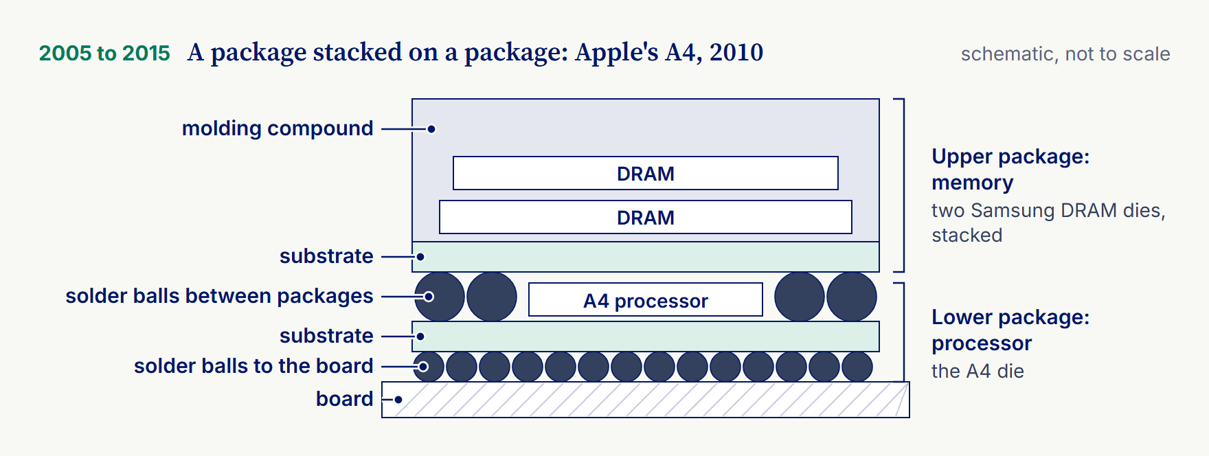
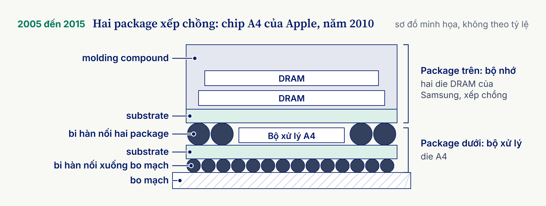
The memory goes on top because it exchanges data only with the processor, so its connections can run through the processor’s package below. Stacked straight above, it sits close to the processor, and the pair takes up the board space of one chip. The processor, which also needs many connections to the rest of the device, keeps the lower package and its grid of balls to the board.
Bộ nhớ nằm ở trên vì nó chỉ trao đổi dữ liệu với bộ xử lý, nên các kết nối của nó có thể đi qua package của bộ xử lý ở bên dưới. Khi xếp chồng ngay phía trên, bộ nhớ nằm sát bộ xử lý, và cả cặp chỉ chiếm diện tích bo mạch của một con chip. Còn bộ xử lý, vốn cần nhiều kết nối với các phần khác của thiết bị, giữ package phía dưới cùng lưới bi hàn nối xuống bo mạch.
Chapter 4 turns the die itself face down, so that it, too, meets its package across its whole face.
Chương 4 lật úp chính con die xuống, để nó cũng nối với package trên khắp bề mặt của mình.